>K9m 2013, TOM 143, Bbin. 1, cTp. 158 165
© 2013
DISTORTIONS OF THE COULOMB BLOCKADE CONDUCTANCE LINE IN SCANNING GATE MEASUREMENTS OF InAs NANOWIRE
BASED QUANTUM DOTS
A. A. Zhukova* Ch. Volkh'c, A. Windenh>c, H. Hardtdegenhc, Th. Schäpersh'c'd
" Institute of Solid State Physics, Russian Academy of Sciences 142432, Chernogolovka, Moscow Region, Russia
bPeter Grimberg Institut (PGI-9), Forschungszentrum Jülich 52425, Jülich, Germany
JARA-Fundamentals of Future Information Technology, Forschungszentrum Jülich
52425, Jülich, Germany
dII. Physikalisches Institut, R.WTH Aachen Universität 52056, Aachen, Germany
Received February 28, 2012
We performed measurements at helium temperatures of the electronic transport in the linear regime in an InAs quantum wire in the presence of a charged tip of an atomic force microscope (AFM) at low electron concentration. We show that at certain concentration of electrons, only two closely placed quantum dots, both in the Coulomb blockade regime, govern conductance of the whole wire. Under this condition, two types of peculiarities — wobbling and splitting — arise in the behavior of the lines of the conductance peaks of Coulomb blockade. These peculiarities are measured in quantum-wire-based structures for the first time. We explain both peculiarities as an interplay of the conductance of two quantum dots present in the wire. Detailed modeling of wobbling behavior made in the framework of the orthodox theory of Coulomb blockade demonstrates good agreement with the obtained experimental data.
DOI: 10.7868/S0044451013010158
1. INTRODUCTION
During the last decade, measurements of the conductance of low-dimensional systems using a charged AFM tip as a mobile gate (scanning gate microscopy measurements or SGM measurements) proved to be a powerful and efficient method. Using this technique, different types of micro- and nanostructures have been investigated such as quantum point contacts fl 3], quantum rings [4], and quantum dots based 011 hetero-junctions [5 7], graphene [8, 9], carbon nanotubes [10 12], and InAs nanowires [13, 14].
While experiments 011 carbon nanotubes did not result in essentially new effects (the potential profile along the nanotubes was measured in [10] and the stability of the 4-fold energy level degeneracy against
* E-mail: azhukovfl'issp.ac.ru
long-range Coulomb potential disturbances was confirmed in [12]), several unexpected experimental results 011 quantum dots based 011 graphene have been obtained [8, 9]. The presence of bound states in the contact constriction regions was shown and, additionally, wobbling and splitting of the Coulomb blockade conductance line [8, 9] were observed. While the splitting of the Coulomb blockade conductance lines was explained as the crossing of the state of two neighboring dots [8, 9], the mechanism of the wobbling of these lines remains unclear.
One of the problems to be solved before any speculations 011 the physical mechanism of the observed effect is the correct interpretation of the results of SGM measurements. The initial statement that SGM experimental results are intuitively clear is not always correct; for example, both splitting gates served to form the structure under investigation [15] and charged dielectric dirt 011 the conductive tip [6] result in additional artifacts
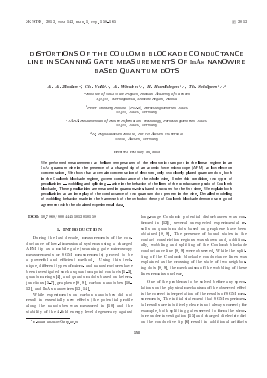
Fig. 1. Scanning electron microscope image of the InAs wire. The source and drain contact pads are marked by "S" and "D". The scale bar corresponds to 2 pm. The rectangle represents the area of the scanning gate measurements at helium temperature. The position of the tip during the transport measurements (Vsd vs Vbg) is marked by an asterisk
in the SGM experimental data. Thus, not only the explicitly interpreted experimental SGM data but also additional simulations and model calculations of the SGM measurements are absolutely necessary fC, 15].
In this paper, we present SGM experimental results measured in an InAs quantum wire at helium temperature. Wobbling and splitting of the Coulomb blockade conductive lines are observed. The obtained experimental results are interpreted within a model that involves two quantum dots connected in series. Calculations focused on the wobbling behavior of SGM scans in the framework of the orthodox theory of Coulomb blockade for different mutual capacitive couplings between two dots are also presented.
2. EXPERIMENTAL
The InAs undoped nanowirc used in our experiment was grown by selective-area metal organic vapor-phase epitaxy [16]. The wire diameter is 100 mil. For our transport measurements, the wire was transferred to an '/¿-type doped Si (100) wafer covered by a 100 mil thick SiO-2 insulating layer. The doped silicon substrate serves as the back gate. The evaporated Ti/'Au contacts to the wire and the markers of the search pattern were defined by electron-beam lithography. The
distance between the contacts is 3.5 //in. A scanning electron microscopy image of the sample under investigation is presented in Fig. 1; the rectangle marks the area of the scanning gate measurements.
The measurements were performed at T = 4.2 Iv. The charged tip of a home-built scanning probe microscope [IT] is used as a mobile gate during scanning gate imaging measurements. We left the tip 300 mil above the SiO-2 surface, in order to eliminate any mechanical or electrical contact of the tip with the InAs wire or metallic contacts. All scanning gate measurements were performed keeping the potential of the scanning probe microscope tip (VL) and the backgate voltage (Vbg) constant. The electrical circuit of the scanning gate imaging measurements is presented elsewhere [12].
3. EXPERIMENTAL RESULTS
The conductance of the wire during the scan and the conductance as a function of the source-to-drain voltage (Vsd) and Vbg is measured in a two-terminal scheme by using the standard lock-in technique. Here, a driving AC voltage with the amplitude Vac = 0.1 niV at a frequency of 231 Hz is applied while the current is measured with a current amplifier.
The wire conductance map as a function of Vsd and Vbg is presented in Fig. 2. The tip voltage V. = 4 V is applied during this experiment. The position of the tip is marked by an asterisk in Fig. 1. The experimental data revealed a quite complex Coulomb diamond structure, which is typical for system of two or more quantum dots connected in series [18, 19, 13]. Formation of dots in the quantum wire occurs because of defects in the wire crystal structure.
Figure 3 presents the set of the scanning gate measurements performed with the constant tip voltage V. = 4 V. Here, the backgate voltages were increased successively from Vbg = 0-89 V (Fig. 3a) in steps of 10 niV to the final value Vbg = 1-06 V (Fig. 3r). This set of SGM measurements demonstrates the formation of two quantum dots in the InAs wire connected in series. Some asymmetry of the scanning gate imaging pictures is due to the nonpcrfcct shape of the AFM tip. The centers of the two observed dots are placed approximately 350 mil apart, as can be seen in the enlarged scan shown in Fig. 4a.
The set of experiments presented in Fig. 3 was intended to reveal the formation of the double-dot structure in the most explicit way and to eliminate any suspicions about the possibility of a more complex structure realized in the InAs nanowirc in the relevant range of backgate voltages. With increasing the backgate
VSD, mV
Fig. 2. Conductance map measured at 4.2 K as a function of the source-to-drain voltage and backgate voltage. The double Coulomb blockade pattern reveals the presence of at least two quantum dots connected in series. The applied tip voltage is
v, = 4 V, the tip position is marked by the asterisk in Fig. 1
Fig. 3. Series of scanning gate measurements of the InAs nanowire measured from Vbg = 0.89 V to 1.06 V in steps of 10 mV. The tip voltage is kept constant at 4 V. Brighter areas correspond to a higher conductance. In (a), the positions of dots 1 and 2 are respectively marked with grey and white circles. Coulomb blockade conductance lines with wobbling (in (n) and (r)) are marked with arrows. The scale bar corresponds to 1 pm for all images
voltage, dot 1 (the left one in Fig. 3) starts to be filled with electrons, then dot 2 (the right one) starts to be occupied with electrons. As dot 2 is filled with electrons, the resistance of the InAs nanowire decreases below 100 MQ. In Fig. 3«, the wobbling of the Coulomb blockade conductive line of dot 2 occurs for the first time at Vbg = 1-02 V. Subsequently, with increasing the backgate voltage, the wobbling is suppressed (Fig. 3o q) and then revives at Vbg = 1-06 V, as can be seen in Fig. 3r. To reveal the interplay of the conductance of both dots, Fig. 4a reproduces Fig. 3« with additional dashed lines corresponding to the lines of conductance minimums of dot 1 (grey) and lines of conductance peaks of dot 2 (white).
Figure 46 shows a scanning gate measurement made at V. = 4 V and Vbg = 1-40 V. It is clearly seen that at the higher backgate voltage, a new feature, the splitting of the Coulomb blockade conductive lines, is observed (marked with arrows) in addition to the wobbling of the Coulomb blockade conductive lines. A similar behavior of the Coulomb blockade conductance lines was
observed in a graphene-based quantum dot [9]. In [9], the splitting of the Coulomb blockade conductance lines was interpreted as the crossing of the state of two neighboring dots with mutual Coulomb interaction, but the wobbling of the Coulomb blockade conductance lines was not explained.
4. THEORETICAL SIMULATIONS OF SGM MEASUREMENTS AND DISCUSSION
The main aim of simulations in framework of the orthodox theory of Coulomb blockade is to confirm the statement that the physical mechanism of wobbling is based on the interplay, revealed with SGM of the conductance of two quantum dots connected in series (see Figs. 3 and 4). To show the influence of the parameters of the quantum dots on
Для дальнейшего прочтения статьи необходимо приобрести полный текст. Статьи высылаются в формате PDF на указанную при оплате почту. Время доставки составляет менее 10 минут. Стоимость одной статьи — 150 рублей.