ОПТИКА И СПЕКТРОСКОПИЯ, 2010, том 108, № 2, с. 255-259
КВАНТОВАЯ ИНФОРМАТИКА. ^^^^^^
КВАНТОВО-ИНФОРМАЦИОННЫЕ ПРОЦЕССЫ
УДК 535.14
ENGINEERING SILICON-BASED PHOTONIC CRYSTAL CAVITIES FOR NV-CENTER QUANTUM INFORMATION PROCESSING
© 2010 C. A. Foell*, A. M. Zagoskin******, and J .F. Young*
*Department of Physics and Astronomy, The University of British Columbia, Canada **Frontier Research System, RIKEN, Japan ***Department of Physic, Loughborough University, United Kingdom E-mail: foell@phas.ubc.ca
Received August 3, 2009
Abstract—Silicon slab photonic crystal microcavities designed for off-resonant coupling to nitrogen vacancy (NV) centers were simulated and fabricated. FDTD-simulations show the partial density of states spectrally near the NV-center electric dipole transition can be tuned to reduce decoherence of an excited NV-center despite this transition being above the silicon electronic band gap. The partial density of states at the NV-cen-ter transition can be made to dip below half of the free-space partial density of states without significantly affecting the cavity mode quality factor. These promising results sustain the merits of using silicon as a base photonic crystal material for quantum information processing even when integrated emitters radiate above the electronic band gap of silicon.
INTRODUCTION
Nitrogen vacancy (NV) centers in diamond have seen recent growth in interest from the quantum optics, quantum information processing (QIP), and quantum computation communities due in part to their remarkable, optically-accesible spin coherence properties at room temperature [1]. Optical accessibility allows for the spin quantum coherence in the ground state of an NV-center to be transferred to photonic degrees of freedom, which in turn act as "flying qubits" — long-distance carriers of quantum information in both theoretical large-scale quantum computing [2, 3] and commercially realized quantum communication schemes [4]. The photonic degrees of freedom available to interact with the NV-centers can be engineered by placing them in photonic crystal mi-crocavities with high quality factors (Q-factors) and small mode volumes, that can be efficiently coupled to low-loss optical waveguides.
Of existing base materials for photonic crystal structures, silicon has been shown to support cavities with Q values greater than 2 x 10⁶ [5], sufficient for many quantum information processing schemes involving NV-centers. Unfortunately silicon absorbs at the NV-center dipole transition frequency (470 THz), strongly limiting the performance of silicon-based cavities operating at this frequency. This has motivated research that seeks to realize high Q microcavities in materials transparent at the NV-centre transition frequency. One candidate is diamond itself [6], but relevant fabrication techniques rely on relatively slow focused ion beam methods, and published Q values for these cavities are only of order 103 [7]. A class of wide
band-gap alternatives are the chalcogenide glasses, which have recently overcome reliance on focused ion beam patterning in favor of the relatively speedy electron beam patterning technique [8], and Q values of over 104 have been experimentally realized [9]. Thirdly, interest in silicon nitride (SiN) has grown, as evidenced by recent coupling of diamond nanoparticles to a SiN-based photonic crystal of Q on the order of several thousands [10], and unpublished simulation work by an independent group reporting SiN-based cavities for coupling to diamond nanoparticles with Q values in excess of 2 x 10⁵ [11].
Although recent advances in nanofabrication of these three materials have been made, none offer the highly desirable ability to directly integrate with silicon-based technology. With the aforementioned limitation of silicon absorbing at the NV-center dipole transition, a potential workaround would be to fabricate cavities operating at a lower frequency (below the silicon electronic band gap), place a NV-containing diamond nanoparticle inside the silicon cavity, and couple the two off-resonantly. Quantum information processing schemes involving coupling of an electronic qubit to a sharp, off-resonant photonic mode have been proposed [12], including a two-qubit gate that effectively couples two NV-centers via a single mode [13]. However, one potential drawback in coupling optical centers with dipole transitions above the electronic band gap of the resonator base material is the possibility that this would increase the dephasing rate of the transition.
In this report we simulate dipole emitters operating at the NV-center transition placed inside silicon-
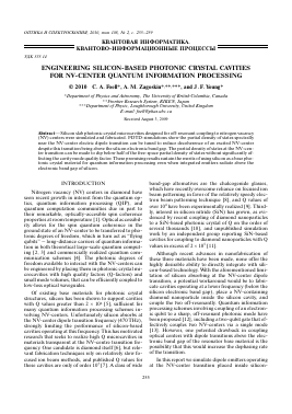
Cavity schematic SEM image of fabricated cavity
Fig. 1. (a, b, c) — geometry for photonic density of states calculation, point dipole sources are positioned in the center of the central hole, orientation of sources are indicated by arrows (in and out of page for z-oriention), a time-domain electric field monitor — indicated by a "X" — is placed at the source location, simulation spatial extent indicated by bounding rectangle; (d, e) — cavity design (described in text).
based photonic crystal cavities with specifically cavities with a central air hole in which a diamond nano-particle could be placed. We tune cavity parameters to simultaneously achieve two ends: reduce the photonic density of states near the NV-center transition at 470 THz to minimize deleterious dephasing, and establish a cavity mode with high Q values and low mode volumes. We report structures based on 200 nm thick Si slabs with a partial density of states for oriented dipole transitions at 470 THz that are actually a factor of two less than free space, when the dipole is located in the centre of an air hole cavity with Q values on order 7000.
MODEL
Cavity modes and density of states (DOS) curves were engineered using FDTD simulations (FDTD Solutions, Lumerical). Density of states calculations followed the Green dyadic approach as implemented for example in [14]. The local DOS can be expressed in terms of the imaginary part of the Green function tensor for the electric field which can in turn be extracted from time-domain electric field monitors positioned near point dipole sources [15]. This was implemented by including a point dipole source at the cavity center in one of three orientations (Figs. If— 1c). The partial density of states was calculated for each dipole orientation at the cavity center.
CAVITY DESIGN, MODES
Integration of diamond nanoparticles containing NV-centers with high Q disk-shaped microresonan-tors [16], microsphere resonators [17—19], and photonic crystal cavities [10] have been reported in all cases by placing the nanoparticles on the surface of the material that confines the light. This approach does not place the dipole transition at the peak field of the mi-crocavity. An improvement for diamond nanoparticle integration would involve placing the nanoparticle at the mode maximum, which would require a cavity with a mode maximum in air, something that is possible using photonic crystal cavities. While it would remain a challenge to locate the nanoparticles in the "air holes" of such a cavity, a number of routes are currently being pursued, such as nanoparticle trapping with optical-mode-induced dipole forces [20].
To explore this type of cavity, we choose a design (Figs. 1d, 1e) with a central air hole based on one proposed and investigated in a different context by Vuck-ovic et al. [21]. The defect consists of four modifications to a uniform hexagonal photonic crystal: (a) radial reduction of a central defect hole to a radius rcen, (b) radial reduction of the four holes nearest the central defect hole on the rJ symmetry axes to a hole radius rrj, (c) elongation by an amountp in the x-direc-tion of the holes lying on the y axis (y-axis running through the central defect), and (d) shifting of the 'TJ holes" away from the central defect hole and along the rJ symmetry axes by an amount Arj.
Cavities investigated possessed parameters rcen/a = = 0.18, Arj/a = 0.05, rrj/a = p/a = 0.05, hole radius r/a = 0.25 for lattice pitch a. A pitch of a = 440 nm yields a photonic bandgap that brackets the 1.5 ^m telecommunication window. The slab thickness was fixed to coincide with that of the silicon on insulator photonic crystals typically fabricated in our laboratory (200 nm), although larger slab thicknesses can yield larger Q values ([21] and simulations performed for this work).
For these parameters, a typical cavity supports two high Q modes with strong mode concentration in the central cavity air hole [21, 22]: one x-oriented dipole and one y-oriented dipole state. A second x-dipole mode lying spectrally above the y-dipole mode is localized outside the central defect hole in the silicon, and is consequently less suitable for coupling to an NV-center (i.e., in nanodiamond form). Mode volumes of less than 0.1 (V2)3 and Q values of several thousand are typical for the x-dipole mode, which consistently has a higher Q than the y-dipole mode and the second x-dipole mode. The highest Q value simulated was 7000 for the localized x-dipole mode with 11 rings of holes around the central defect, a corresponding y-dipole Q of 5000, and a second x-dipole Q of 3000. Example intensity profiles are provided in Fig. 2.
Although a Q value of 7000 is sufficient for some emitter-cavity coupling applications it falls short for most quantum information processing schemes particularly those involving NV-centers. The two-qubit gate involving two NV-centers coupled to a common off-resonant cavity mode proposed by Zagoskin et al. [13] demands a Q value in excess of 2 x 10⁵. Previous studies of this particular type of defect [22, 23] suggest that the Q values of the first x-dipole mode could be limited to of order 104 (maximum value of 3 x 10⁴ for similar parameters considered here, but thicker photonic crystal slabs). As the purpose of the present work was primarily t
Для дальнейшего прочтения статьи необходимо приобрести полный текст. Статьи высылаются в формате PDF на указанную при оплате почту. Время доставки составляет менее 10 минут. Стоимость одной статьи — 150 рублей.