Pis'ma v ZhETF, vol.93, iss. 10, pp.665-668 © 2011 May 25
Femtosecond pulse crystallization of thin amorphous hydrogenated films on glass substrates using near ultraviolet laser radiation
V. A. Volodin1), A. S. Kachko+, A. G. Cherkov+, A. V. Latyshev+*, J. Kochv, B. N. Chichkovv +A.V. Rzhanov Institute of Semiconductor Physics RAS, 630090 Novosibirsk, Russia * Novosibirsk State University, 630090 Novosibirsk, Russia v Laser Zentrum Hannover, 30419 Hannover, Germany
Submitted 15 March 2011 Resubmitted 11 April 2011
Femtosecond laser treatments (second harmonic of Ti-sapphire laser, A « 400 nm wavelength, < 30 fs pulse duration) were applied for crystallization of thin hydrogenated amorphous silicon films on glass substrates. The concentration of atomic hydrogen in the films was varied from 10 to «35%. The energy densities (laser flu-ences) for crystallization of the films with thicknesses from 20 to 130 nm were found. Assumedly, non-thermal processes (plasma annealing) take place in phase transition caused ultra-fast pulses. The developed approach can be used for creation of polycrystalline silicon films on non-refractory substrates.
The interest in amorphous silicon films on non-refractory substrates and their crystallization is constantly stimulated by demands of giant microelectronics. For example, enlargement of sizes of flat panel displays with active thin film transistor matrix can be described as "reverse Moor's low". Modern techniques of deposition allow producing of hydrogenated amorphous silicon (a-Si:H) films on substrates with plasticity temperature as low as 100 °C. For some applications the polycrystalline silicon films have many advantages comparing with a-Si:H films. So, the development of low thermal budget technology of crystallization of a-Si:H films is actual, and is of interest up today, especially for femtosecond laser crystallization [1-5]. Femtosecond laser treatments also used for creation of nanocrystals in dielectric films [6,7] and for silicon nanostructuring [8]. But near-infrared laser radiation was mainly used for crystallization [1-7]. Near ultra-violet radiation has higher absorption for a-Si:H films, so, lesser laser fluence will be need to crystallize the films, and lesser radiation can reach substrate, what important for crystallization of very thin films.
Thin a-Si:H films were deposited on non-refractory glass substrates (temperature of plasticity « 300 °C) using low-temperature plasma enhanced chemical vapor deposition (PECVD) technique. The growth temperature was varied from 200 to 280 °C, the thickness of the films was varied from 20 to 130 nm. It is known, that optical gap of a-Si:H depends on hydrogen concentration [9]. According to optical gap measurements from light transmission and reflection data, the films grown at
e-mail: volodin0isp.nsc.ru
temperature 280 °C contain 10-15 atomic % of hydrogen (optical gap «1.5eV); the films grown at temperature 200 °C contain 30-35% of hydrogen (optical gap « 2 eV).
A Ti-Sapphire laser (FemtoPower Compact Pro, Femtolasers Produktions GmbH) with a central wavelength of 800 nm, pulse duration of < 30 fs, pulse energy of up to 0.8 mJ and pulse repetition rate of 1 kHz was used for laser treatments. The pulse energy was set using a computer controlled polarization rotating LCD device in front of the laser's prism based pulse compressor. To make laser treatments in near ultraviolet range, the non-linear optic crystal for generation of second harmonic of this laser was used. The pulse energy of second harmonic can be varied up to 10 /¿J. The laser beam was focused onto the sample surface using an achromatic lens. The radius of the laser spot was changed in a range from 50 to 500 micrometers by defocusing. The distribution of the laser energy in the laser spot has the Gaussian form:
E(r) = E0eM^r2/r20), (1)
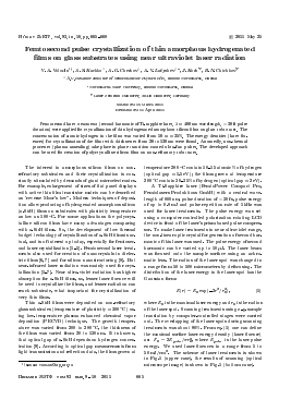
where E0 is the maximal laser energy and ro is the radius of the laser spot. Scanning treatments using »-y-sample translation by computer-controlled stages were carried out. The overlapping of the laser spots during scanning treatments was about 90%. From eq. (1) one can define the maximal surface laser energy density (laser fluence) as: F0 = 2Epnise/irrl, where Epnise is the laser pulse energy. We used laser fluences in a range from 5 to 50mJ/cm2. The scheme of laser treatments is shown in Fig. 1 (upper case), the results of scanning (optical microscope image) is shown in Fig. 1 (bottom case).
ÜHCbMa b ?K3T<J> tom 93 Bbin.9-10 2011
665
666
V. A. Volodín, A. S. Kachko, A. G. Cherkov et al.
Focusing lense
A
Stage 4
Area with content of silicon nanocrystals И Я
S
Lase r CO И
s
a-Si:H
Fig. 1. Upper case: scheme of laser treatments; bottom case: optical microscope image of laser scanned sample, darker areas are polycrystalline Si
Raman spectroscopy technique was used to identify the structure (amorphous or crystalline) of the films. The Raman spectra were recorded in the back-scattering geometry. The 514.5 nm Ar+ laser line was used as a source. Triple spectrometer (T64000 Horiba Jobin Yvon) with a micro-Raman setup was used. All Raman spectra were measured at room temperature. To avoid heating of the films, the laser beam was slightly defocused leading to a spot diameter of about 6 /tm at a laser power reaching the sample of 2-3 mW.
The Raman spectrum of amorphous silicon contains broad peaks at approximately 480 cm-1 appearing as result of effective density of transversal optical (TO) vibration modes [10]. Due to scattering on optical phonon modes localized in the nanocrystals, the Raman spectrum of nanocrystals is characterized by narrow peak at position between 500-520 cm-1. The position and the width of the peak strongly depend on size and structure of the nanocrystals according to dispersion of the localized modes [11]. The peak width is mainly determined by size dispersion of the nanocrystals. The intensity of the "nanocrystal" peak depends on the contents of
nanocrystal phase. So, one can determine the volume part of nanocrystal phase:
^nano — Si/Vfuii = Inc/{Inc + ctIa), (2)
where Imc and 1a are integral intensities of nano-crystalline and amorphous peaks, and a is relation between the integral Raman cross sections of nanocrystal Si and a-Si. According to literature data, a can change from 0.1 for large grain polycrystalline silicon up to 1.1 for nanocrystalline Si [12].
According to Raman spectroscopy data, the femtosecond laser treatments (second harmonic of Ti-sapphire laser, А и 400 nm wavelength, <30fs pulse duration) with fluence less than 20mJ/cm2 have not changed the structure of the a-Si:H films. As one can see in Fig. 2 the femtosecond laser impacts with fluence higher than 20mJ/cm2 lead to dramatic changes in structure of the a-Si:H film with 10-15% of hydrogen. For laser impact with fluence 25mJ/cm2 one can see amorphous peak (480 cm-1) and appearing of nanocrystalline peak with maximum at 515 cm-1. In the case of laser impact with fluence 30 mJ/cm2 the amorphous
Письма в ЖЭТФ том 93 вып. 9-10 2011
Femtosecond pulse crystallization of thin amorphous hydrogenated
667
^ 600
QJ сл сл
1
о 400
0
1 200 e
400 420 440 460 480 500 520 540 Raman shift (cm )
Fig. 2. Raman spectra of the films with relatively low hydrogen concentration: solid line - as deposited sample; dashed and doted lines poly-Si films (after femtosecond laser impact). Insert - schematic process of Auger generation
peak is small compared with nanocrystalline peak, so one can conclude that the film almost totally crystallized. As it was mentioned, from position of this peak one can estimate the average size of Si nanocrystals. In this case the average size is about 5nm. The ablation threshold for femtosecond pulse treatments for near ultraviolet photons in this case was 35mJ/cm2. Earlier, in the case of femtosecond laser pulse treatments near IR range the ablation threshold for a-Si:H film with 10-20% of hydrogen was found to be of about 65 mJ/cm2 [4].
In the case of a-Si:H film with 30-35% of hydrogen the crystallization threshold is much higher. As one can see in Fig. 3, laser treatment with fluence 40mJ/cm2
^ 300
О QJ сл сл
§ 200
о
ХУ
§ 100 "S
400 420 440 460 480 500 520 540 Raman shift (cm 1)
Fig. 3. Raman spectra of the films with relatively high hydrogen concentration: solid line - as deposited sample; dashed and doted lines poly-Si films (after femtosecond laser impact)
leads only to partly crystallization of the film. It should be noted, that the film thickness in this case was several times lesser (20 nm versus 130 nm in the case of a-Si:H
Письма в ЖЭТФ том 93 вып. 9-10 2011
film with 10-15% of hydrogen). When laser fluence was 25mJ/cm2 and lower, no structural changes were observed in the highly hydrogenated films. Supposedly, the dependence of needed for crystallization laser fluence on concentration of hydrogen is caused by difference in absorbance coefficient owing to hydrogen [9].
For very short time of pulse, the absorbed energy cannot dissipate in substrate, so, knowing the heat capacity and specific heat of melting for a-Si, one can easy calculate the energy density needed for total melting of a film. According to data [4] the energy density needed for total melting of a-Si:H film with thickness 130 nm is 76mJ/cm2. So, if assume the thermal mechanism of crystallization, the laser fluence 30mJ/cm2 is not enough to melt this film. We assume some non-thermal effects. The pulse duration is much lower than time of electron-phonon interaction in semiconductors (about 1-2 picoseconds). So, hot electron-hole plasma can not excite vibration modes in material during pulse. The excitation of an electron from valence band to conduction band means a break of a valence bond. According to some theoretical calculations, when from 9 to 20% valence bonds are broken, silicon became unstable [3,13]. According to estimations of Bok [14], when concentration of excited electron-hole pairs reaches
Для дальнейшего прочтения статьи необходимо приобрести полный текст. Статьи высылаются в формате PDF на указанную при оплате почту. Время доставки составляет менее 10 минут. Стоимость одной статьи — 150 рублей.