Pis'ma v ZhETF, vol. 100, iss. 1, pp. 34-41 © 2014 July 10
Investigations of local electronic transport in InAs nanowires by scanning gate microscopy at helium temperatures
A. A. Zhukov+1\ Ch. Volk*x, A. Winden*x, H. Hardtdegen*x, Th. Schäpers*xo Institute of Solid State Physics of the RAS, 142432 Chernogolovka, Russia
* Peter Grünberg Institut (PGI-9), Forschungszentrum Jülich, 52425 Jülich, Germany
x JARA-Fundamentals of Future Information Technology, Forschungszentrum Jülich,
52425 Jülich, Germany
°II. Physikalisches Institut, RWTH Aachen University, 52056 Aachen, Germany
Submitted 29 May 2014
In the current paper a set of experiments dedicated to investigations of local electronic transport in un-doped InAs nanowires at helium temperatures in the presence of a charged atomic-force microscope tip is presented. Both nanowires without defects and with internal tunneling barriers were studied. The measurements were performed at various carrier concentrations in the systems and opacity of contact-to-wire interfaces. The regime of Coulomb blockade is investigated in detail including negative differential conductivity of the whole system. The situation with open contacts with one tunneling barrier and undivided wire is also addressed. Special attention is devoted to recently observed quasi-periodic standing waves.
DOI: 10.7868/S0370274X14130074
1. Introduction. In the past decade considerable interest was devoted to investigations of electronic transport of individual one-dimensional mesoscopic systems such as carbon nanotubes (CNT) and nanowires (InAs, InN) [5, 1, 6, 7, 8, 4, 2, 3]. Usually, for such experiments field-effect transistors are fabricated from individual one-dimensional (ID) objects by forming metallic contacts by electron-beam lithography. The highly doped Si substrate is used as a gate to alter the main parameters such as the carrier density and the opacity of the tunneling barriers in the metallic contacts to ID object interfaces. The issue of contact opacity at the interfaces is extremely important. In fact, it may change the whole scenario from well defined Coulomb blockade [9] in case of closed contact tunneling barriers to Fabry-Perot interference for almost opened contacts [10].
Generally speaking, one-dimensional systems are rather different and may have as ballistic [10] so diffusive dominating transport as in InAs [5-8] or InN nanowires [4]. Additionally, crystal structure defects may result in the formation of tunneling barriers dividing the tube or wire into sequentially connected quantum dots and by that suppress the conductivity of the whole system dramatically [11]. Thus, the ability of altering of the potential profile locally and influence the density of carriers in ID system locally is rather desirable.
-^e-mail: azhukov@issp.ac.ru
One viable ways to realize such local impact on a ID system is to create a set of side- or top-gates along the nanowire or nanotube [12]. A more versatile and elegant method which became popular in the past decades is to use a charged tip of an atomic-force microscope as a mobile gate, so-called scanning gate microscopy (SGM). Using SGM different types of low-dimensional micro-and nano-structures have been investigated: quantum point contacts [13-15], quantum rings [16], and quantum dots based on heterojunctions [17-19], graphene [20], and carbon nanotubes [21-23]. The additional benefit of this technique is the resulting clear and easy reading and intuitively understandable images of quite high resolution (up to 100 nm), thus shedding light on internal local structure of system under investigation.
In the current manuscript a set of SGM experiments, performed on InAs nanowires at T = 4.2 K, is presented. Experiments are carried out at different carrier densities, different opacities of the contacts and on wires with different numbers of internal tunneling barriers. Thus, a wide range of scenarios from closed sequentially connected quantum dots demonstrating Coulomb blockade to metallic diffusive wire are realized and investigated. Special attention is devoted to induced negative differential conductance (NDC) [24] and recently observed quasi-periodic oscillations [25, 26].
This article is organized as follows: in section 2 experimental details are described, in section 3.1 experi-
mental results obtained on InAs nanowires in Coulomb blockade regime are presented and discussed, section 3.2 is dedicated to experiments investigating recently observed quasi-periodic oscillations and the conclusion is made in section 4.
2. Experimental details. In all our experiments we study nominally undoped InAs nanowires grown by selective "cirGcl metal-organic vapor-phase epitaxy [27]. The diameter of the wires is 100 nm, typically. The wire is placed on an n-type doped Si (100) substrate covered by a 100 nm thick SiC>2 insulating layer. The Si substrate serves as a back-gate electrode. The evaporated Ti/Au contacts to the wire as well as the markers of the search pattern were defined by electron-beam lithography. The distance ¿w¡re between the contacts varies for different samples from 1.5 to 3.5 /xm. A scanning electron beam
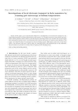
Fig. 1. (a) - Scanning electron micrograph of the typical InAs wire with metallic contacts. The source and drain contact pads are marked by "s" and "d". The horizontal scale bar corresponds to 1 /mi. The metallic triangle on the left side of the wire is a marker of the search pattern, (b) - Electrical circuit of the scanning gate microscopy measurements. The back-gate voltage Vbg is applied to the doped Si substrate while the tip voltage Vt is applied to the tungsten tip of the probe microscope. The resistance of the wire is measured using a two terminal circuit by applying a current (Iac) and measuring the voltage (V). From Ref. [25]
micrograph of the typical sample is shown in Fig. la. The source and drain metallic electrodes connected to the wire are marked by S and D.
Investigations of grown InAs wires by transmission electron microscopy demonstrate that the wires are usually covered by a 2-nm-thick oxide layer [5]. In order to create good ohmic contacts to wire, this oxide must be removed. But even with such precautions some residual Schottky-like potential barriers may be observed even at room temperatures [28]. These barriers becomes essentially less visible at high back gate voltages and this behavior is quite similar to one on the interface of CNT and Pd metallic contacts [9].
Письма в ЖЭТФ том 100 вып. 1-2 2014
All measurements presented in this paper are performed at T = 4.2 K. In our experimental setup we have several parameters which can been changed independently such as the tip voltage (Vt), the back gate voltage (Vbg) and the position of the tip, see Fig. lb. Additional parameters dedicated to measurements of the conductance of the wire in a two-terminal circuit are source-to-drain DC voltage and driving AC current/voltage. The measurements are done by using a standard lock-in technique. If the wire demonstrates strong Coulomb blockade regime an AC driving voltage is applied and the resulting current is measured. In the opposite case of open contacts a driving AC current is applied, while the voltage is measured by a differential amplifier. The detailed values of the driving AC voltage and current are adjusted for a certain experimental setup and sample, and can be found elsewhere [24-26, 30,31].
In the SGM experiments the charged tip of a home-built scanning probe microscope [29] is used as a mobile gate during scanning gate imaging measurements keeping the potential of the scanning probe microscope tip as well as the back-gate voltage and driving AC current/voltage constant. Another type of experiments presented here (see section 3) is based on the frozen tip position and tip voltage while Vbg and DC source-to-drain voltages are swept for mapping of the conductance Vsd vs. Vbg typical for measurement in the Coulomb blockade regime.
An additional parameter in SGM experiments is the tip to Si02 surface distance. Its crucial effect on the sample conductance and thus on resulting experimental SGM images will be discussed in detail in section 3.2.
3. Experimental results and discussion. 3.1. Electronic transport in nanowires with defects: Coulomb blockade regime. In this section a set of experimental results obtained in InAs nanowires containing one or more tunneling barriers is presented and discussed. Generally speaking, the potential profile of InAs wire along the wire axis is not flat even if the wire lies on the thin (100 nm) SiC>2 layer and the screening from the back-gate is quite comprehensive. Essential crystal structure defects result in the tunneling barriers of different opacities. The opacity of the barriers increases with increasing the back-gate voltage. This happens partially because the decreasing widths of depletion regions arranging the barrier from both sides. Some of barriers may produce nonlinear transport even at quite high back-gate voltages (Vbg = 7.5 V) (Fig. 3b in [30]).
If the opacity of barrier is low the wire becomes divided into sequentially connected quantum dots demonstrating Coulomb blockade at T = 4.2 K. Detailed inves-
3*
tigations of electronic transport of such InAs nanowires in linear and non-linear transport regimes with scanning gate microscopy were investigated in detail in Refs. [30, 31] and [24], correspondently.
For a more comprehensive understanding of the influence of the charged AFM tip on the wire it is useful to discuss results of calculations made in the orthodox Coulomb blockade model [32] following Ref. [31]. In this model the InAs wire is considered to be divided into two sequentially connected quantum dots. The next main parameters are used to characterize this system: dot 1(2) to back-gate capacitance (Ci(2)bg)? the mutual capacitance of the dots (Cm), and the capacitance of dot 1(2) to the left (right) contact (C^^), the width of the energy levels
Для дальнейшего прочтения статьи необходимо приобрести полный текст. Статьи высылаются в формате PDF на указанную при оплате почту. Время доставки составляет менее 10 минут. Стоимость одной статьи — 150 рублей.