Pis'ma v ZhETF, vol.95, iss.ll, pp.653-658
© 2012 June 10
Surface acoustic wave controlled charge dynamics in a thin InGaAs
quantum well
F. J. R. Schülein, J.Pustiowski, K. Müller*, M.Bichlerx, G. Koblmüllerx, .T.J.Finhn . A. Wixforth,
H. J. Kreimer
Lehrstuhl für Experimentalphysik 1 and Augsburg Centre for Innovative Technologies (ACIT), Universität Augsburg, 86159 Augsburg,
Germany
Center for NanoScience CeNS, 80539 München, Germany x Walter Schottky Institut and Physik Department, Technische Universität München, 85748 Garching, Germany
Submitted 23 April 2012
We experimentally study the optical emission of a thin quantum well and its dynamic modulation by a surface acoustic wave (SAW). We observe a characteristic transition of the modulation from one maximum to two maxima per SAW cycle as the acoustic power is increased which we find in good agreement with numerical calculations of the SAW controlled carrier dynamics. At low acoustic powers the carrier mobilites limit electron-hole pair dissociation, whereas at high power levels the induced electric fields give rise to efficient acousto-electric carrier transport. The direct comparison between the experimental data and the numerical simulations provide an absolute calibration of the local SAW phase.
Over the past 15 years surface acoustic waves (SAWs) have proven to be a powerful and versatile tool to control the electronic and optical properties of semiconductor nanostructures at radio frequencies up to several gigahertz [1-5]. One prominent example is the dissociation of photogenerated excitons and the transport of the dissociated electrons (e's) and holes (hJs) at the speed of sound within the plane of a quantum well (QW) [6, 7]. This peculiar effect arises from the band edge modulation induced by the SAW generated electric fields in piezoelectric materials and can be observed also in one-dimensional systems such as embedded quantum wires [8] or isolated nanowires [9]. Until now, the dynamics of this SAW driven process have been studied mainly in the limit of low SAW amplitudes [10, 11]. However, for high SAW amplitudes, i.e strong piezoelectric fields, a transition from a regime at which the low mobility of fc's limits the efficiency of this process to a fully field-driven regime is expected [12]. While for low SAW amplitudes optical emission is modulated at the fundamental SAW frequency /saw, in the field-driven regime this periodicity is expected to double providing a characteristic fingerprint.
Here, we report on the direct spectroscopic study of SAW controlled emission modulation and its dynamics spanning the entire range of SAW amplitudes and resolving the transition from mobility limited (low amplitudes) to field-driven (high amplitudes) dissociation of photo-generated (e-h) pairs in a thin, disordered QW.
e-mail: hubert.kreimerôphysik.uin-augsburg.de
We resolve a characteristic transition of the emission modulation and its dependence on the local SAW phase which we find in good agreement with numerical simulations of the underlying drift and diffusion current equations [12]. We find that such complete SAW power and phase scans of the optical emission provide a direct calibration of the absolute local SAW phase.
Our sample was grown by molecular beam epitaxy (MBE) on a semi-insulating GaAs (100) substrate. After growth of a GaAs buffer layer, we deposit a 100 nm Alo.7Gao.3As sacrificial layer for subsequent wet chemical etching. On top of this sacrificial layer, the optically active layer is grown which consists of a 220 nm GaAs buffer, 4 ML Ino.5Gao.5As and a 280 nm GaAs capping layer. During the growth of the the InGaAs layer, the substrate rotation was stopped to form a gradient of the In coverage which results in the formation of self-assembled quantum dots (QDs) in regions of high coverage and a thin wetting layer (WL) without QDs in the low coverage region [13]. For the experiments presented here, we are exclusively focusing on material for which only a WL is present and no QDs are nucleating. Thus, we ensure that we resolve the SAW-dynamics of a thin and disordered QW formed by the InGaAs WL without carrier capture into fully confined QD levels superimposed. These layers are epitaxially lifted off the GaAs susbtrate by selective wet chemical etching using hydrofluoric acid in an established process [2,14,15] and transferred on a 128° rot YX LiNb03 host substrate. On this highly piezoelectric crystal SAWs can be excited ail-electrically by interdigital transducers (IDTs)
ÜHCbMa b ?K3T<J> Tom 95 Bbin.11-12 2012
653
654
F. J. R. Schiilein, J. Piistiowski, K. Müller et a1.
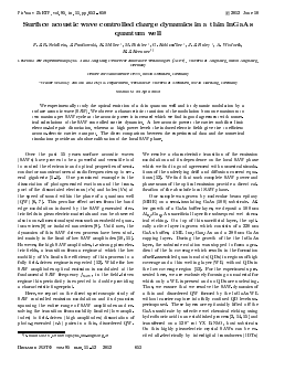
with a more than one order of magnitude increased efficiency compared to GaAs. A schematic of the final device is shown in Fig. la which allows for excitation of
Fig. 1. (a) - Schematic of hybrid SAW device consisting of a LiNbOs chip with an IDT to generate a SAW and an epitaxially transferred GaAs-based heterostructure. (b) -Type-II band edge modulation induced by a SAW leading to a spatial separation of e's and h's. (c) - Electric potential $ (line) and electric field orientation (F) at (x = 0) (arrows) as a function of the local SAW phase (<p)
Rayleigh-type SAWs with a wavelength Asaw = 40 /tm corresponding to a frequency /saw = 98 MHz (Tsaw = 10.2 ns). The strain and electric fields accompanying the SAW in the LiNb03 substrate extend to the optically active semiconductor layers as the total thickness of the semiconductor film of 500 nm is ~ 80 times smaller than the acoustic wavelength. All optical experiments are carried out at T = 10 K in a liquid Helium flow cryostat in a conventional /¿-photoluminescence (PL) setup. For the optical excitation, we use an externally triggered pulsed laser diode emitting ~ 60 ps long pulses at 661 nm with
500 nW time averaged power. The laser beam is focused onto the sample by a 50 x objective to a ~ 2/tm diameter spot and the emitted PL is collected by the same objective. The PL signal dispersed by a 0.5 m grating mono-chromator is analyzed using a Si single photon avalanche diode (SPAD). In order to resolve the full SAW-driven dynamics of the PL even using time-integrated detection, we employ a phase-locked, stroboscopic excitation scheme [16] for which we actively phase-lock an rf signal generator to excite the SAW and a pulse generator to trigger the laser diode by setting n/iaser = /saw with n integer. With this technique, we are able to tune the laser excitation over two full SAW cycles by tuning the relative phase < ip < +27r of the RF signal which generates the SAW.
The SAW induced piezoelectric fields lead to a type-II band edge modulation in the QW which leads to a dissociation of photo generated e-h pairs. At sufficiently high acoustic powers the two carrier species can be transferred to their respective stable points in the conduction and valence band which are separated by half the acoustic wavelength, thus suppressing their radiative recombination [6]. This is shown schematically in Fig. lb. At a fixed point in space, the electric potential # oscillates as the local SAW phase ip tunes over 27r. As depicted in Fig. lc, the resulting electric field F gyrates with two characteristic maxima of its lateral component at ip = 0,2ir and ip = ir where the in-plane component of |V#| is maximum. At these characteristic values of ip field-driven processes are expected to dominate [12] giving rise to two minima of the QW emission per SAW cycle which become observable at high SAW amplitudes.
In Fig. 2a we present the measured PL emission intensity of the QW as a function of the RF power, —41 dBm< PRF < 27 dBm, applied to the IDT and the (local) SAW phase ip tuned from r to +27r. As the RF power is increased, the emission shows the characteristic quenching behavior due to the dissociation of e-h pairs and the resulting inhibition of their radiative recombination. At fixed Prf the emission exhibits oscillatory behavior as ip is tuned. At low Prf < ^20 dBm, we observe a modulation with one maximum per SAW cycle (i.e. two maxima over the 47r range studied here). As Prf increases, a second oscillation with two maxima per cycle sets in and becomes more prominent at higher RF power levels. To further analyze this data we plot ip scans at selected characteristic RF power levels in Fig. 2b. In this data, we identify four regimes:
(i) for smallest acoustic powers below ^40 dBm (black square/line) no pronounced modulation is resolved;
IlHCbMa b ?K3T<1> tom 95 Bim. 11-12 2012
Fig. 2. (a) - Intensity map of the QW PL as a function of the acoustic power and relative phase, (b) - Five representative phase scans over two SAW cycles (—2tt < ip < 2ir) at constant SAW powers (symbols) and fits of eq. (1) (lines) demonstrating the transition from one maximum to two maxima per SAW cycle, (c) - Simulated SAW intensity modulation (lines) corresponding to the experimental data
(ii) at small SAW powers, ^40 dBm < Psaw <
< ^25 dBm (red bullet/line online) we observe a weak
< 10% peak-to-peak modulation with the fundamental period of the SAW. Moreover, the overall intensity increases compared to no SAW excited. Here, the band edge modulation induced by the SAW is weak and, therefore, the finite mobilities of e's and ft's are limiting the carrier transport;
(iii) in the intermediate power range (green up triangle/line and light blue down triangle/line online),
25 dBm < Psaw < 10 dBm, two modulations of the emission are superimposed. In addition to the aforementioned modulation with one maximum, a second oscillation with two maxima per SAW cycle is clearly resolved. This additional modulation becomes more pronounced with increasing RF power pointing towards the predicted transition to fully field-driven carrier dissociation and transport;
(iv) at the highest power levels accessible, Psaw > > 10 dBm, field-driven processes dominate and the overall emission is almost completely quenched. Most notably, the two characteristic maxima
Для дальнейшего прочтения статьи необходимо приобрести полный текст. Статьи высылаются в формате PDF на указанную при оплате почту. Время доставки составляет менее 10 минут. Стоимость одной статьи — 150 рублей.