Pis'ma v ZhETF, vol. 95, iss. 6, pp. 336 - 342 © 2012 March 25
The c-axis charge traveling wave in coupled system of Josephson
junctions
Yu. M. Shukrinov+V, M. Hamdipour+* + BLTP, Joint Institute for Nuclear Research, 141980 Dubna, Russia *Institute for Advanced Studies in Basic Sciences, P.O.Box 45195-1159, Zanjan, Iran
Submitted 11 January 2012 Resubmitted 6 February 2012
We demonstrate a manifestation of the charge traveling wave along the c-axis (TW) in current voltage characteristics of coupled Josephson junctions in high-Tc superconductors. The branches related to the TW with different wavelengths are found for the stacks with different number of Josephson junctions at different values of system's parameters. Transitions between the TW branches and the outermost branch are observed. The electric charge in the superconducting layers and charge-charge correlation functions for TW and outermost branches show different behavior with bias current. We propose an experimental testing of the TW branching by microwave irradiation.
Many physical and biological objects may be considered as coupled nonlinear oscillators [1]. Particularly, intrinsic Josephson junctions (J J) in high temperature superconductors are studied from this point of view often [2]. An attractive feature of intrinsic J J is a generation of coherent radiation in terahertz region and this feature is investigated intensively today [3, 4]. A coupling between junctions plays an important role: it leads to multiple branch structure in the current voltage characteristics (CVC) which have the additional in compare with single junction case features like the breakpoint (BP) current, the BP-region width and the transition currents between branches [7, 6, 5, 8]. It was shown that the BP in CVC is a manifestation of the parametric resonance in this system when the Josephson oscillations create a standing longitudinal plasma wave perpendicular to the superconducting layers. The parametric resonance features were observed experimentally recently [9].
A well known feature of single long Josephson junction is the traveling wave along the barrier [2]. It was noted [10, 11] that the system of capacitively coupled JJ has a plane wave which corresponds to the longitudinal Josephson plasma propagating perpendicular to the junctions. The sharp resonance peak in the microwave absorption spectrum obtained in Bi-2212 by Matsuda et al. [12] has been identified with this collective Joseph-son plasma mode. Instability of the longitudinal plasma oscillations was discussed in [11] and it was proposed that the multiple branches are caused by the freezing of the collective LPW into the static charge density wave.
In this letter we demonstrate the additional branch in CVC of coupled JJ which corresponds to the charge traveling wave along c-axis when the junctions are in rotating states (phase differences are not small). Such branches were not investigated before. Transitions in hysteresis region from the outermost branch (OB) to the traveling wave branch (TWB) and between the TWB with different wavelengths are found. We demonstrate the appearance of the TWB at I = Ic as well which originates from different branches of CVC including the zero voltage branch. A different dynamics of correlation functions for the TWB and for the OB is shown. We find the effect of the microwave irradiation on TWB, which allows the experimental testing of this branch.
To simulate the CVC we investigate the phase dynamics in the framework of the capacitively coupled Josephson junctions with diffusion current (CCJJ+DC) model [13-15], which is determined by the system of dynamical equations
dir t ■ adW
d i/ dt^1 = Vl
a(Vl+1 + Vi-i - 2Vt)
(1)
(2)
e-mail: shukrinv0theor.jinr.ru
for the gauge-invariant phase differences <fii(t) between superconducting layers (S-layers). Here a and ¡3 are the coupling and dissipative parameters, relatively, time t is normalized to the inverse plasma frequency w^1 (u}p = 2eIc/hC), the voltage - to the value Vq = Hu}p/2e, the current - to the critical current I = Ic. The question concerning the value of capacitive coupling constant in real materials is still open. In [16] the authors estimated
I
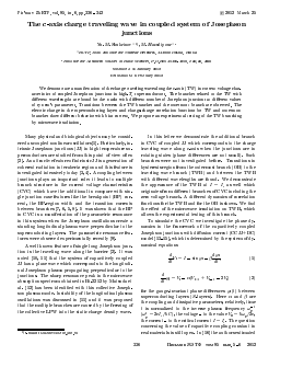
Fig. 1. (Color online) Manifestation of the TWB in CVC of the stacks with 10 JJ. The insets enlarges the parts of CVC: (a) -near transition from the OB to another branch; (b) - calculated in the framework of the CIB-model with nonequilibrium parameter rj = 0.1 and the same other parameters; (c) - near transition at I = 1 (I = Jo), where the TWB is created
it in interval (0.1-5.0) for layered superconductors. The features described in our paper are not sensitive to the value of coupling parameter. To compare our results with previous publications we put а = 1. Using the Maxwell equation div(ee0i?) = Q, where £o is the permittivity (electric constant), we express the charge density
Qi = Qoa(Vl+1 - Vt) (3)
in the S-layer I by the voltages Vi and Vi+1 in the neighboring insulating layers, where Qo = eeo^o/rb- We consider the periodic boundary conditions in this paper. The structure of the simulated CVC in the CCJJ+DC-model is equidistant in agreement with the experimental results [17]. The details of simulation procedure are presented in [8, 18].
The manifestation of the TWB is shown in Fig. 1, where we present the total branch structure of CVC for the stack with 10 coupled JJ at а = 1, 0 = 0.2. It was obtained by multiple sweeping of the bias current through the stack [19, 7, 8]. This CVC is characterized by switching all junctions to the rotating (R) state at I = Ic, large hysteresis, and multiple branching in the
hysteresis region by switching the JJ to the oscillating (O) states with a decrease of the bias current.
The inset (a) enlarges the part of CVC corresponding to the transition from the OB to the another branch. As we can see, there is one more branch additionally to the OB. We prove below that this is the TWB. Such TWB was manifested in CVC of the stack with 10 JJ in [7] (see Fig. 5), but it was not discussed at that time. We would like to stress that TWB in CVC is not a specific for CCJJ+DC-model only. Inset (b) shows the part of CVC-calculated in the framework of the charge imbalance (CIB) model [13, 20] with nonequilibrium parameter t] = 0.1 and the same other parameters. We see that it demonstrates the TWB as well, which is marked by arrow in the figure. The detailed description of the CVC, TWB and breakpoint features related to the CIB-effect will be presented somewhere else.
To see the origin of TWB we investigate first a transition region in CVC near Ic. In during of the sweeping bias current procedure we observe the jumps to the OB and TWB both from the zero voltage state directly and from the other branches of CVC. The inset (b) enlarges the part of CVC corresponding to this transition region.
V 40
38
36
- (а) N14 PBS а =1.0 TWB k^ND OB
ß = 0.2
TWB 40.2 У 40
- X 2 = ND/2
д /----
39.8 - V,
1 1 0.5772 . I ,
0.54 0.56 0.58
I
80 - (b) N28 \ OB = А,0
V а =1.0 А* — A. Q/2
ß = 0.2
78
76 1 A, = Jt0/4у
74 "Г..... 1
0.54
10 20 Layer's number
0.16 Qi 0.08 л A* Ajq/2 т\ г \ - т \ т \ • • • •
0 7 /
-0.08 г Vе
-0.16' V ' *.............
10 20 Layer's number
0.56 I
0.58
10 20 Layer's number
-0.1 0 0.1 Ô/-1
Fig. 2. (Color online) Demonstration of the TWB corresponding to the traveling waves with different wavelength, (a) - The manifestation of the TWB for the stack with 14 JJ. Inset demonstrates the transition from the OB to the first TWB with A = 14D. (b) - The same for the stack with 28 JJ. (c) - The distribution of the charge in S-layers along the stack with 28 JJ for TWB with A = Ao at bias current I = 0.577. (d) - The same for A = A0/2. (e) - The same for A = A0/4. Figures (f)-(h) show the corresponding Lissajous charge-charge diagrams
The TWB in the CVC have been observed in the stacks with different number of junctions. Particularly, the TWB were found in the stacks with 14 JJ and 28 JJ (Fig. 2), 9 JJ (Fig. 3d) and 7 J J (Fig. 4). In case of even number of junctions in the stack, the jump from the OB to the TWB happens first to some unstable state. Such transition for stacks with 14 JJ at a = 1, 0 = 0.2 is demonstrated in the inset (a) to Fig. 2, where the transition from the parametric resonance region of OB is observed. For the stacks with odd number of junctions we
observe usually the jumps to the TWB from the chaotic part of breakpoint region in the OB. The increase of bias current after jump instead of its decrease allows us restore the total TWB (see Fig. 3).
We note that the longest wavelength of a TW in the system with N J J is Ao = ND, where D is a period of lattice (the sum of thicknesses of insulating and superconducting layers). So, the waves with A = ND¡n might appear in the stack, where n is devisor of number N. We stress that the TWB in Fig. 1 was naturally
TWB (c)
(BVtnp ~ P/iV=
= 3.912 1
5 , 10
0.78 0.79
0.81 0.82
Fig. 3. (Color online) Manifestation of the TWB in CVC of the stack with 9 JJ at a = 3, ¡3 = 0.2 and periodic BC. The insets (a) and (b) show the charge oscillations in two 5-layers at I = 0.792 in OB and TWB, relatively. The inset (c) presents the results of FFT-analysis of charge oscillations for TWB at 1 = 0.792
obtained just by sweeping of bias current. Another possibility is to use the variation of the initial conditions for phase differences. In Fig. 2 we show such realization of the TWB corresponding to TW with different wavelengths. Particularly, in Fig. 2a we demonstrate the manifestation of the TWB in CVC of the stacks with 14 JJ related to the waves with Ao = 141? and A = Ao/2. Inset demonstrates a transition of the OB to the first TWB with A = Ao- The analysis of the time dependence of the charge in S-layers and its distribution along the stack around the second transition in Fig. 2a shows that the TW with A = A0 transforms
Для дальнейшего прочтения статьи необходимо приобрести полный текст. Статьи высылаются в формате PDF на указанную при оплате почту. Время доставки составляет менее 10 минут. Стоимость одной статьи — 150 рублей.