Pis'ma v ZhETF, vol. 93, iss. 2, pp. 101 -104 © 2011 January 25
Charge density wave transport in NbSe3 at low temperatures under
high magnetic field
Yu. I. LatyshevA. P. Orlov, P. Monceau+* Kotelnikov Institute of Radio-Engineering and Electronics RAS, 125009 Moscow, Russia + Neel Institute, CNRS, 38042 Grenoble, France * Laboratoire National des Champs Magnetiques Intenses at Grenoble, CNRS, 38042 Grenoble, France
Submitted 9 December 2010
Charge density wave (CDW) depinning and sliding regimes have been studied in NbSe3 at low temperatures down to 1.5 K under magnetic field of 19 T oriented along the c-axis. We found that the threshold field for CDW depinning becomes temperature independent below To « 15 K. Also CDW current to frequency ratio characterizing CDW sliding regime increases by factor 1.7 below this temperature. The results are discussed as a crossover from thermal fluctuation to tunneling CDW depinning at T < To. Besides, we found that CDW sliding strongly suppresses the amplitude of Shubnikov-de Haas oscillations of magnetoresistance.
NbSe3 is a one of the most conventional material for studies of charge density wave (CDW) sliding regime. CDW dynamics is well documented in this material at high temperatures, above 30 K [1]. To the contrast, the low temperature CDW dynamics in Nbse3 is nearly unstudied. That is related mainly with a fact that the threshold electric field Et (or voltage Vt) for CDW depinning exponentially grows up with a decrease of temperature [2], while the electric resistance of the sample R drops down. Therefore, that is rather difficult to achieve threshold voltage at low temperatures avoiding Joule heating of the sample which is proportional to V2 ¡R. In a present paper we developed some experimental improvements to reduce heating effects. First, we studied CDW transport under high magnetic field which considerably, by factor of 10 at H = 20 T and T = 1.5 K, increases sample resistivity. Additionally, we used pulsed technique with current pulse width as short as 100 ns and high duty factor. Using those improvements we achieved CDW depinning and sliding regimes at low temperatures under conditions of highly eliminated heating effects.
The interest to the low temperature CDW dynamics in NbSe3 is related with a possibility of macroscopic quantum tunneling of CDW in the impurity potential predicted by Bardeen [3] that is expected to be realized at low temperatures [4,5]. Another interesting point is to study the effect of CDW sliding on Shubnikov-de Haas (ShdH) oscillations of magnetoresistance [6].
The experiments have been carried out on high quality NbSe3 samples with residual resistance ratio above 100. The samples have been placed on sapphire sub-
e-mail : yurilatyshev0yahoo.com
strate and covered by collodion to improve thermal contact with the substrate. The measurements of the I-V characteristics and their derivatives have been done by 4 probes method using computer controlled DC current source and nanovoltmeter. Pulsed measurements have been done with a use of generator of signals with a digitizing rate of 2 GHz and "LeCroy WR104Xi" oscilloscope with a band width of 1 GHz and digitizing frequency of 10 GHz. The measuring system allowed to measure resistance on current pulses of length less then 100 ns with a duty factor above 103. The measurements in high magnetic fields up to 21T have been done in Grenoble National Lab of High Magnetic Field.
Figs, la, b show two sets of differential I-Vs measured below 60 K down to 4.2 K. The threshold voltage Vt is characterized by sharp decrease of dV/dl with voltage. One can see that below 44 K Vt starts to increase rapidly up from 1 mV to about 6 mV at 33 K and then remains nearly unchanged with further temperature decrease down to 26 K. At lower temperatures the differential resistance below threshold rapidly drops down (Fig.lb) and below 12 K the dV/dI(V) curves transform into wider curves with threshold of about 30 mV which again is nearly non-changed below 12 K down to 1.5 K. The temperature dependence Vt (T) is plotted in semilog scale in Fig.lc. One can see that in average this dependence well follows exponential law Vt oc exp(^T/T0) found by Coleman et al. [2], but more detailed dependence shows two plateaus below 30 and 14 K.
As is well known, the CDW sliding is accompanied by narrow band noise (NBN) with a frequency proportional to the CDW velocity. The ratio of the CDW current to the NBN frequency is a constant characterizing sliding regime. The NBN frequency can be determined
IlHCbMa b ?K3T<J> tom 93 Bbin. 1-2 2011
101
102
Yu. I. Latyshev, A. P. Orlov, P. Monceau
Fig.l. Sets of the differential I-Vs dV/dI(V) measured at temperature intervals 60-26K (a) and 24-4 K (b) and temperature dependence of threshold voltage Vt of NbSe3 sample #3 under magnetic field of 19 T, H || c. The straight line corresponds to the exponential dependence Vt oc exp(^T/To) [2] with To « 15 K. The threshold voltage has been determined on the level of one half of the total height of dI/dV(V = 0) — dl/dV (V Vt). Note that for some temperatures (T = 24^12 K) one can see two jumps of dI/dV(V), corresponding to two thresholds.
120 100 80 60 40 20 0
f = 900 MHz
-4 -2
(b) 2.0
■
Vrf (mV) сл 1.5 -
-0 § ■
-150
-180 -fi 1.0 -
-210 S3 ■
-240 ■
0.5 -
■
2 4 0
I (mA)
H = 19 T, H||c (c) f = 0.9 GHz
J_I_I_I_I_L
10 20 30 40 T (K)
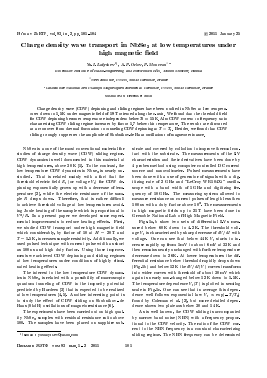
Fig.2. Shapiro step spectra of NbSe3 sample #3 in magnetic field of 19 T oriented parallel to the c-axis at 4.2 K (a) and 20 K (b) under RF-radiation with frequency of 900 MHz. For the panel (a) RF-power is increased from top to bottom and curves are shifted down for clarity. Panel (c) shows the ratio of CDW current to frequency at various temperatures extracted from Shapiro step data at H = 19 T, H || c-axis
directly from noise spectra or indirectly by observation of so-called Shapiro steps on the I-V characteristics under RF-field [1]. Shapiro steps appear when the frequency of external RF-field fex matches NBN frequency. Fig.2a show Shapiro step spectra of NbSe3 sample under RF-field with a frequency of 900 MHz at 4.2 K. The top curve corresponds to the zero RF power. The threshold feature at I = 1.7 mA is clearly seen. With an increase of the RF power from top to bottom the threshold decreases and Shapiro steps develop as the peaks on dV/dI(I) spectra. Observation of Shapiro steps provides a direct evidence of CDW sliding at low temperatures. For a comparison Fig. 2b shows similar Shapiro spectra at 20 K. One can see that at high enough RF-power the spacing between zeroth, first and second peaks become equal and saturates with power. This fundamental value, A I, defines a current value which CDW carry
by displacement on its one period for one cycle of the external frequency [1]. The ratio Д/ to fex is a constant associated with a charge of the one period of CDW.
A temperature dependence of this ratio (Fig.3c) is generally flat having some jump at temperature T0 « и 15 К, below which the ratio increases by factor of 1.7. Amazingly, that dependence Vt(T) also changes at that point and becomes nearly flat at lower temperatures. Therewith, this value, T0 = 15 K, appears in the "averaged" exponential dependence of Vt(T) at temperatures above 15K. All these findings indicate that the temperature T0 is some characteristic temperature with different regimes of CDW pinning and sliding above and below To.
At low temperatures CDWs in NbSe3 coexist with the uncondensed carriers localized at the pockets of the Fermi surface where the nesting condition for the CDW
Письма в ЖЭТФ том 93 вып. 1-2 2011
Charge density wave transport in NbSe3 at low temperatures under high magnetic held
103
a ß;
50
40
30
20
10
12
16
11
10
9
8
7
6
5 20
H (T)
T =4.7 K
^ DC
J — w = 500 ns
-w = 200 ns
:....... (b) 1 , 1
0 4 8 12 16 20
1 ^ 10
£
OJ T3
"E
I
1 r
4
(mA)
Fig.3. The variation of magnetoresistance of NbSe3 sample #3 at 1.5 K at various DC currents indicated in the plot (a), the insert shows correspondent dI/dV(V) dependence at this temperature under magnetic field H = 19 T, H || c. A comparison of magnetoresistance measured under DC and pulsed currents with duration of w = 500 ns and 200 ns of 9mA(b) and a dependence of the amplitude of ShdH oscillation A at H = 12 T upon the DC current value above the threshold current for CDW depinning It = 1.7mA (c). The straight line corresponds to the exponential law A oc exp /It)
0
4
8
6
wave vector is not achieved. At low temperatures in high magnetic fields the spectrum of these free carriers becomes quantized. That manifests itself as ShdH oscillations of the magnetoresistance in NbSe3. The pinned CDW does not affect essentially pocket carriers, while sliding CDW can increase their scattering and even drag them. In that case one can expect remarkable influence of CDW sliding on ShdH oscillations. There is only one paper [6] where ShdH oscillations have been studied in NbSe3 at high currents, however, neither a threshold for the CDW sliding no heating effects have been clearly defined there. Here we justified a regime of CDW sliding at low temperatures by observation of sharp threshold voltage behaviour of the I-V characteristics and Shapiro step response to the RF-field. Fig.3a demonstrates a set of R(H) dependences at various DC currents at 1.5 K, while the insert to Fig.3a shows the dV/dI(I) at this temperature to show the current region for CDW sliding.
At low currents R(T) dependences well reproduced behaviour that has been studied earlier [2,6]. With current growth the oscillations become damped, first, slightly starting with currents of 0.5 mA and then more strongly at currents above 2 mA. Note that positions of minimums of oscillations do not change remarkably.
The insert to Fig.3a shows that the complete CDW depinning happens at 1.7 ma while some partial depinning accompanied by spikes on dV/dI(I) occurs
Для дальнейшего прочтения статьи необходимо приобрести полный текст. Статьи высылаются в формате PDF на указанную при оплате почту. Время доставки составляет менее 10 минут. Стоимость одной статьи — 150 рублей.