Pis'ma v ZhETF, vol. 101, iss. 1, pp. 44-49 © 2015 January 10
Conductance oscillations at the interface between a superconductor and the helical edge channel in a narrow HgTe quantum well
A. Kononov+1\ S. V.Egorov+, N. Titova*, Z.D.Kvonx, N. N. Mikhailovx, S. A. Dvoretskyx, E. V. Deviatov+° + Institute of Solid State Physics of the RAS, 142432 Chernogolovka, Russia * Moscow State Pedagogical University, 119991 Moscow, Russia x Institute of Semiconductor Physics, 630090 Novosibirsk, Russia ° Moscow Institute of Physics and Technology, 141700 Dolgoprudny, Russia Submitted 26 November 2014
We experimentally investigate electron transport through the interface between a superconductor and the edge of a two-dimensional electron system with band inversion. The interface is realized as a tunnel NbN side contact to a narrow 8 nm HgTe quantum well. It demonstrates a typical Andreev behavior with finite conductance within the superconducting gap. Surprisingly, the conductance is modulated by a number of equally-spaced oscillations. The oscillations are present only within the superconducting gap and at lowest, below IK, temperatures. The oscillations disappear completely in magnetic fields, normal to the two-dimensional electron system plane. In contrast, the oscillations' period is only weakly affected by the highest, up to 14 T, in-plane oriented magnetic fields. We interpret this behavior as the interference oscillations in a helical one-dimensional edge channel due to a proximity with a superconductor.
DOI: 10.7868/S0370274X15010099
Recently, a strong interest appears to the investigations of electron transport through the interface between a superconductor (S) and a normal (N) semiconductor-based low-dimensional structure. Because of the Majorana problem [1], this interest is mostly connected with different SNS type structures, where the N region is a one-dimensional quantum wire [2-7] or a topological surface state [8, 9].
An attractive example of a one-dimensional topological surface state is a current-carrying helical edge channel, realized in a narrow HgTe quantum well [10]. This channel originates if the well thickness exceeds the critical 6.3 nm due to the inverted band structure in the bulk HgTe two-dimensional system [11-14]. In contrast to the conventional quantum Hall edge states [15], this channel is helical, i.e. it consists of two spin-resolved counter-propagating states in zero magnetic field. Despite the initial idea of a topological protection [10,12-14], backscattering appears at macroscopic distances [16, 17], possibly due to the allowed two-particle process [18] and to the electron puddles [19]. The edge current has been directly demonstrated in a visualization experiment [20] in zero magnetic field. Also, the supercurrents have been investigated for a two-terminal SNS Josephson junction, with a rectangular
-^e-mail: artemk23@mail.ru
section of quantum well located between two superconducting leads [9]. So, a narrow HgTe quantum well is a promising candidate [21] for the search for a topological superconductivity [22, 23].
On the other hand, even a single SN interface is predicted to demonstrate a number of intriguing effects, e.g. conductance oscillations due to a proximity effect [24, 25], giant spin rotation [26], and localized edge states [27]. Pronounced Fabry-Perot oscillations have been demonstrated for a three-dimensional Bi2Se3 topological insulator sandwiched between a superconducting and normal leads [28]. In this experiment, a proximity with a superconductor doubled the period of the oscillations, although they were present also for normal leads. Thus, it seems to be reasonable to investigate electron transport in a single SN side contact at the edge of a narrow HgTe quantum well.
Here, we experimentally investigate electron transport through the interface between a superconductor and the edge of a two-dimensional electron system with band inversion. The interface is realized clS cl tunnel NbN side contact to a narrow 8 nm HgTe quantum well. It demonstrates a typical Andreev behavior with finite conductance within the superconducting gap. Surprisingly, the conductance is modulated by a number of equally-spaced oscillations. The oscillations are present only within the superconducting gap and at
lowest, below 1K, temperatures. The oscillations disappear completely in magnetic fields, normal to the two-dimensional electron system plane. In contrast, the oscillations' period is only weakly affected by the highest, up to 14 T, in-plane oriented magnetic fields. We interpret this behavior as the predicted [25] interference oscillations in a helical one-dimensional edge channel due to a proximity with a superconductor.
Our Cdo.65Hgo.35Te/HgTe/Cdn.65Hgo.35Te quantum well with [013] surface orientation and width d = 811111 is grown by molecular beam epitaxy. A detailed description of the well structure is given elsewhere [29, 30]. Because d exceeds the critical value 6.3 11111, the quantum well is characterized by band inversion [16, 17]. It contains a two-dimensional electron gas (2DEG) with the electron density 1.5-1011 cnr2 and the low-temperature mobility 2 • 105 cm2/Vs, as obtained from standard magnetoresistance measurements.
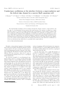
A sample sketch is presented in Fig. 1. A 20011111 high mesa step is formed by dry etching in Ar plasma.
Fig. 1. (Color online) Sketch of the sample (not in scale) with electrical connections. The 100 /u.m wide mesa has two In Ohmic contacts (yellow). The 20/u.m wide superconducting NbN stripe (gray) is placed at the mesa step, with low (2-3 jL/m) overlap. Because of the insulating layer on the top of the structure, a side SN junction is formed between the NbN electrode and the 2DEG edge at the mesa step. We study electron transport across one particular NbN-2DEG junction in a three-point configuration: a current is applied between one of the In Ohmic contacts and a superconducting NbN electrode which is grounded while the other In contact measures the 2DEG potential. Because of the relatively low in-plane 2DEG resistance and the low resistance of the superconducting NbN electrode, the measured dV/dI(V) curves reflect the behavior of the NbN-2DEG interface
We fabricate two Ohmic contacts to the 2DEG by annealing In. In addition, we use dc magnetron sputtering to deposit a 50 11111 thick superconducting NbN film at the mesa step, the surface is mildly cleaned by Ar plasma before sputtering. To avoid any 2DEG degradation, the sample is not heated during the sputter-
ing process. The 20 ¿«11 wide NbN stripe is formed by lift-off technique, with low (2-3 ¿«11) mesa overlap, see Fig-1.
Because of the insulating layer on the top of the structure, a side SN junction is formed between the NbN electrode and the 2DEG edge at the mesa step. In samples with etched mesa an insulating region of finite width is always present at the 2DEG edge [31, 32]. In our samples this region is significant enough to provide tunnel S-2DEG junctions, which are characterized by 0.5—1.5 Mil normal resistances Rn-
We study electron transport across one particular NbN-2DEG junction in a three-point configuration: a current is applied between one of the In Ohmic contacts and a superconducting electrode which is grounded (see Fig. 1) while the other In contact measures the 2DEG potential. To obtain dV/d,I(V) characteristics, we sweep the dc current through the interface from —4 to +411A. This dc current is modulated by a low ac (4 pA, 2 Hz) component. We measure both the dc (V) and ac
dV/dl) components of the 2DEG potential by using a dc voltmeter and a lock-in amplifier, respectively. The latter is equipped by a preamplifier with the 100 Mil input impedance. We have checked, that the lock-in signal is independent of the modulation frequency in the 1-6 Hz range, which is defined by applied ac filters.
Because of the relatively low in-plane 2DEG resistance (about 1 kil at present 2DEG concentration and mobility), and the low resistance of the superconducting NbN electrode, the measured dV/d,I(V) curves reflect the behavior of the NbN-2DEG interface. To extract features specific to the HgTe edge transport, the measurements were performed at a temperature of 30mK. Qualitatively similar results were obtained in several cooling cycles, for different absolute values of the junctions' Rn-
The examples of dV/d,I(V) characteristics are presented in Fig. 2a. They demonstrate a behavior, which is qualitatively consistent with a standard Andreev one for a single SN junction [33]. A clearly visible NbN superconducting gap can be determined ANbN = ±1.58 mV (denoted by dashed lines in Fig. 2), which corresponds well to the directly measured critical temperature Tc = = 11 Iv for a similar NbN film.
Within the gap at |eV| < ANbN, the maximum differential resistance Rmax ~ 3 Mil is undoubtedly finite, which is only possible due to the Andreev reflection [33]: if the Andreev process was suppressed, tunnel conductance would be zero at |eV| < ANbN- According to the BTIv theory [33], a single-particle scattering is significant at the SN interface, because Rmax exceeds the normal junction resistance value Rn ~ 0.5 Mil. A corre-
46
A. Kononov, S. V. Egorov, N. Titova et al.
0
V (mV)
Fig. 2. (Color online) (a) - Examples of dV/dI(V) characteristics for a single NbN-2DEG side junction in zero magnetic field at two different temperatures T « Tc = 11 K. The dV/dI(V) curves are of standard Andreev behavior [33]. They demonstrate a clearly visible NbN superconducting gap ANbN = ±f.58mV (denoted by dashed lines), which corresponds well to the directly measured Tc = 11 K. Within the gap at \eV\ < A^n, the maximum differential resistance iîmax is undoubtedly finite. Inset demonstrates a perfect scaling of two low-temperature (30 mK) dV/dI(V) curves for the junctions with different normal resistances Rn (0.5 and 1.5MO respectively), i.e. a constant resistance ratio iîjv/-Rmax ~ 0.16. The pronounced d.V/dl
Для дальнейшего прочтения статьи необходимо приобрести полный текст. Статьи высылаются в формате PDF на указанную при оплате почту. Время доставки составляет менее 10 минут. Стоимость одной статьи — 150 рублей.