Pis'ma v ZhETF, vol. 98, iss. 11, pp. 796-800 © 2013 December 10
Control of the Dirac point in graphene by UV light
A. Yurgens+1), N. Lindvall+, J. Sun+, Y.Nam+*, Y. W.Park* + Department of Microtechnology and Nanoscience (MC2), Chalmers University of Technology, SE-412 96 Göteborg, Sweden * Department of Physics and Astronomy, Seoul National University, 151-747 Seoul, Republic of Korea
Submitted 14 October 2013
It is experimentally shown that the initially shifted Dirac point in graphene-on-dielectric devices can be brought to zero by illuminating the samples with UV light. This is much easier to accomplish compared to the common procedure of annealing at high temperature. Internal photoemission is concluded to be responsible for the observed effect.
DOI: 10.7868/S0370274X13230124
Graphene demonstrates a unique ambipolar field effect: the graphene resistance is a symmetric function of the electric field (the gate voltage Vg). The neutrality (Dirac) point VD of real graphene devices is however seldom at Vg =0 due to extraneous doping from trapped charges in the dielectric [1], adsorbed gases [2], residues of other polar molecules at the graphene surface after processing [3], or water/oxygen redox couple [4] due to unavoidable water layer at the hydrophilic surface of oxidized silicon at ambient conditions. Such surface contaminations and trapped charges give rise to a nonuniform pattern of local electric field, which changes the overall carrier concentration in graphene. This is seen as a shift in the Dirac point along the Vg-scale. The shift can be comparable with the breakdown voltage of the gate dielectric, obviously resulting in unreliable graphene devices. The common way of dealing with this problem is to anneal graphene at temperatures from 200 to 600 °C in vacuum- or inertgas (or hydrogen)-atmosphere, heating either in oven or by current [5]. Annealing removes surface adsorbents and organic residues which results in increased mobilities [6]. However, for graphene on SiO2, for instance, annealing results in a stronger coupling between graphene and dielectric [7]. Graphene then conformally follows the nano-scale roughness of SiO2 surface thereby making graphene locally bent. The increased curvature of graphene makes it susceptible to oxygenation in ambient air [7] leading to hole doping and decrease of mobility [8]. Also, annealing obviously cannot be performed when graphene is used in combination with organic un-derlayers (e.g. polymethylmethacrylate, PMMA) having low melting temperatures.
e-mail: yurgens-at-chalmers.se
In this report, we show that the Dirac point can be more readily shifted to zero by illuminating graphene samples using relatively low-intensity violet/UV-light. The shift can occur in both directions by applying the gate voltage of certain sign during the illumination. This simple technique works for both exfoliated and CVD grown graphene, and also at low temperatures down to - 20-50 K.
Graphene is placed on either 300-nm thick SiO2 obtained by wet oxidation of Si or 90-nm Al2O3 grown by atomic-layer deposition (ALD) on doped Si wafers. The electrodes are patterned by e-beam- or photolithography, and lift-off of Au/Cr double metallization layer. The electrical measurements are made in both two- and four-probe configurations using a small ac excitation current (30-150 Hz, 50-500 nA), and with lock-in amplification of the voltage signal. The gate voltage is applied between one of the current-bias electrodes and doped Si substrate (the back-gate configuration). The range of voltages is dictated by the break-down voltage of the corresponding dielectric, which is found to vary from sample to sample and is detected by monitoring the current through the gate electrode. The Al2O3 gate dielectric is thinner and has higher dielectric constant than the standard 300-nm SiO2 making gate-voltage range « 6.5 times smaller in the former case.
The experiments with illumination are done in a close-cycle cryostat with optical windows. Violet laser with the wavelength A = 405 nm or light emitting diodes (LED's, A > 460) are used to illuminate samples. The effect is largely absent when using LED's with longer wavelengths. The typical light intensities are from 1 to 10 mW/cm2. It is not possible to assure constant intensity for different samples with the present setup.
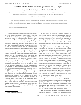
Fig. 1a shows how the Dirac voltage VD of graphene on Al2 O3, initially > 2 V, shifts after illumination done
796
nictMa b X3TO TOM 98 BHn. 11-12 2013
V9 M
3000 -
2000 -
1000 -
a
V-'
20000
15000
10000
5000
Charge density (1016 m 2)
-30 -20
V„(S)
The time evolution of the sample resistance, R(t), is nearly exponential in time, with sometimes two time constants (^20—200s), which depend on both the initial conditions and particular sample. However, no clear pattern of this dependence could be revealed. For the majority of Al2O3-samples, the shift in the Dirac point is reversible. Also, the shift and its time evolution are not symmetric: in some cases it is found that the Dirac point shifts only to negative voltages, irrespective of the gate voltage during the illumination.
It is interesting to note that the charge mobility ^ appears to correlate with the position of Dirac point in the Al2O3-samples. The more negative VD, the higher the mobility (see Fig. 2). The mobility noticeably in-
16 _2
Charge density (10 m )
Fig. 1. (Color online) R(Vg)-curves of graphene on AI2O3/Si substrate at room temperature T = 293 K (a) and graphene on SiO2/Si substrate at T =10 K (b). The arrows indicate shift of the Dirac voltage (corresponding to the maximum of the R(Vg)-curves) after successive illumination doses at Vg =0
at zero gate voltage. It is seen that the curves continuously move in voltage to the left with the Dirac point eventually ending up at Vg « — 1V after « 290 min of accumulated exposure time at « 2 mW/cm2 of light intensity. Similar behavior were reported for high-mobility CVD graphene [9]. This illustrates usefulness of the method for removing (or compensating for) extraneous doping in graphene. Fig. 1b demonstrates that the effect is also present at low temperature. In this case the sample of graphene on SiO2/Si substrate at T = 10 K is measured. The total light-exposure time is 100 min. The intensity of light (« 10 mW/cm2) is several times higher than in Fig. 1a, which might result in excess heating of the sample to an estimated temperature of < 30 K.
0.80
0.75 -
'„ 0.70-
0.65
0.60-
0.55
Fig. 2. The charge mobility ^ versus the Dirac voltage VD for a number of experiments with UV-illumination, when VD is shifted in both directions by applying the gate voltage of certain polarity. Note that after the initial increase, the mobility becomes a reproducible linear function of VD
creases while the Dirac point shifts towards negative voltages immediately after starting the illumination. During subsequent experiments when VD is positive-and then negative again, the mobility becomes a reproducible linear function of VD, although not repeating the initial increase. This indicates that the mobility is at least partly limited by the charged scatterers in the vicinity of graphene [10].
The initial position of the Dirac point VD =0 is obviously caused by some charges or polar molecules in
the vicinity of graphene surface. These can be charges trapped in the oxide layer or molecules adsorbed at the graphene surface and/or interface with underlying substrate. The photoeffect seen in the present- and a few other works [7, 9, 11] is then due to photodesorption of these molecules or neutralization of the trapped charges. Ref. [9] only ascertains the effect of UV-light at room temperature and SiO2, while Refs. [7, 11] focus on the role of molecular oxygen in doping of graphene and only mention the effect of UV-light, without analyzing it in detail or discussing other possibilities.
The mechanism of graphene doping by oxygen [7, 11] does not seem to agree well with our experiments done in helium gas and in a wide range of temperatures. Once being photodesorbed, oxygen molecules are unlikely to diffuse back and be adsorbed altogether again on the small graphene area. During the experiments at cryogenic temperatures, oxygen is much likely to end up being adsorbed at the cold walls of the cryostat. At last, the direction in which the charge-neutrality point moves under UV-light can depend on the polarity of gate voltage during the illumination, which is also impossible to reconcile with the oxygen-doping model.
A layer of water with some oxygen dissolved in it is always present in graphene-on-oxide samples prepared at ambient conditions [12-14]. Oxygen dissolved in water gives rise to O2-water redox reactions involving the transfer of electrons and a few intermediate reactions yielding peroxide (H2O2) and hydroxyl radical (•OH). The latter can form charge traps accumulating a net negative charge at the surface of oxide and attracting a net positive charge to graphene (p-doping). This has very convincingly been demonstrated experimentally in Ref. [4]. The UV-light induced changes can then be associated with the internal photoemission removing trapped electrons possibly resulting in inverse redox reactions. There are however several questions that need to be addressed before ultimately deciding on the very mechanism of the UV-induced changes in graphene doping.
First, assuming that the effect has the same origin for both Al2O3 and SiO2 gate insulators, we note that the conduction-band offset (ECO, see Fig. 3) is probably not important for the observed effect. ECO for SiO2 is slightly larger than the energy of photons of our 405-nm laser (3.06 eV), while it is smaller than that (Eco = 2.4eV) for Al2O3 [15]. This means that if the effect were to include ECO, it would be much stronger in the case of Al2O3. Although indeed, it is somewhat clearer for Al2 O3, the corresponding time scales of the doping change under the illuminat
Для дальнейшего прочтения статьи необходимо приобрести полный текст. Статьи высылаются в формате PDF на указанную при оплате почту. Время доставки составляет менее 10 минут. Стоимость одной статьи — 150 рублей.