Pis'ma v ZhETF, vol. 101, iss. 9, pp. 703-707 © 2015 May 10
Correlations of mutual positions of charge density waves nodes in side-by-side placed InAs wires measured with scanning gate microscopy
A.A.Zhukov^, Ch. Volk+*, A. Winden+*, H. Hardtdegen+*, Th. Schäpers+*x Institute of Solid State Physics of the RAS, 142432 Chernogolovka, Russia + Grünberg Institut (PGI-9), Forschungszentrum Jülich, 52425 Jülich, Germany * JARA-Fundamentals of Future Information Technology, Forschungszentrum Jülich, 52425 Jülich, Germany x II. Physikalisches Institut, RWTH Aachen University, 52056 Aachen, Germany Submitted 31 March 2015
We investigate the correlations of mutual positions of charge density waves nodes in side-by-side placed InAs nanowires in presence of a conductive atomic force microscope tip served as a mobile gate at helium temperatures. Scanning gate microscopy scans demonstrate mutual correlation of positions of charge density waves nodes of two wires. A general mutual shift of the nodes positions and "crystal lattice mismatch" defect were observed. These observations demonstrate the crucial role of Coulomb interaction in formation of charge density waves in InAs nanowires.
DOI: 10.7868/S0370274X1509009X
Essential efforts were made towards investigations of electronic transport in InAs [1-8], InN [9], core/shell GaAs/InAs [10], and Si/Ge [11] nanowires made by bottom-up approach partially because of the rich physics demonstrated by such structures and because of the possible applications of them in electronics and quantum computing. The most experiments done on wires with normal-metallic contacts are dedicated to study magneto-transport properties of field-effect transistors made of nanowires using n-type doped Si substrate as a back gate [1-7,9-11] or PEO/LiCIO solid electrolyte clS cl surrounded gate [8] to alter the number of electrons or holes in the system. These types of measurements reveal the response of the nanowire as the whole masking the local peculiarities of the systems under investigation.
The so called scanning gate microscopy (SGM) technique used the conductive atomic-force microscope tip as a mobile gate became the standard one and helps to reveal the local electronic transport properties of quantum dots [12, 13], quantum point contacts [14-16] or quantum rings [17] based on two-dimensional electron gas or quantum dots based on one-dimensional objects such as nanowires [18-22] and nanotubes [23-25]. The last experiments done on high quality InAs nanowires show a presence of charge density wave (CDW) with wavelength ranges from two-hundred nanometers to one micron formed by electrons of top subband of InAs
-^e-mail: azhukov@issp.ac.ru
nanowire [20]. Detailed SGM experiments help to define three groups of electrons in InAs nanowire [21]: the electrons of top subband, the electrons belonging to "disordered sea" and electrons localized on surface defect centers. These experiments revealed robustness of such charge density wave to application of high source-to-drain voltage, possible coexistence of charge density waves with 2 and 3 nodes and, finally, the splitting of the maxima of charge density wave [21].
Three possible mechanisms of charge density wave formation are considered. The first one is a simple standing waves model [20] excluding formally the influence of charge of the electrons itself on position and wavelength of charge density wave. More cumbersome the second and the third ones are Friedel oscillations and Wigner crystallization formed by Luttinger liquid of electrons in InAs nanowire [26-29]. None of them appear to be suitable to explain charge density wave with micron wavelength [21], but, nevertheless, all three look quite applicable for explanation of charge density wave with wavelengths of hundreds microns. The last experiment [22] demonstrates the presence of slalom-like stable patterns in SGM images interpreted as Wigner crystal instability [26]. This experiment pointed on the principal importance of charge of electrons of top subband on wavelength and charge density wave positions, but more solid evidences look to be necessary to exclude simple standing waves model from consideration.
In the current paper we present a set of experiments made on side-by-side placed InAs nanowires using SGM
IlHCbMa b >K3TO tom 101 Bbin. 9-10 2015
703
704
A. A. Zhukov, Ch. Volk, A. Winden et a 1.
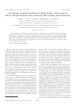
Fig. 1. (a) - Scanning electron micrograph of the InAs side-by-side placed wires with metallic contacts. The source and drain contact pads are marked by s and d. We define the "upper" wire as the one which is shorter on drain side, the other one we define as the "lower". The horizontal scale bar corresponds to 2 /Lim. All scans a,-d have the same scale; b-d are scanning gate microscopy scans made with a tip voltage Vt = 0 V and a back gate voltage of Vbg = —0.2, +0.8, and +3.5 V, corre-spondently. The tip-to-surface distance is maintained at 300 nm. White triangles mark the nodes of charge density waves. The gray triangle in Fig. b notes the beginning of formation of the third node in lower wire. Solid lines and dotted line mark the edges of the metallic contacts and the position of the nanowires. Fig. e shows the dependence of the gaps sizes vs. gaps positions for upper (open squares) and lower (solid circles) wires. The bottom inset is a general scheme of formation of "lattice mismatch" defect in accordance with measured gaps (distances between nodes) sizes. The drain contact position is denoted as "0" /Lim on abscissa in Fig. e
technique. Observable correlations of mutual positions of charge density wave nodes in neighbor wires allow us to reveal the crucial role of charge of electrons in formation of CDW. No essential correlation is found for electrons in "disordered sea" at high electron density (high back gate voltages VBG = (11.0-12.0) V).
In our experiment we study a nominally undoped InAs nanowires grown by selective-area metal-organic vapor-phase epitaxy [30]. The diameter of the wires is 100 nm. The wires were placed on an «-type doped Si(100) substrate covered by a 100 nm thick SiC>2 insulating layer. The «-type doped Si(100) substrate served as the back-gate electrode. The evaporated Ti/Au contacts to the wire as well as the markers of the search pattern were defined by electron-beam lithography. The distance between the contacts is Lw¡re = 3.0 ¿tni. A scanning electron micrograph of the sample is shown in Fig. la.
The source and drain metallic electrodes connected to the wires are marked by s and d. We define the "up-
per" wire as the one which is shorter on drain side, the other one is defined as the "lower" wire.
All measurements were performed at T = 4.2 Iv. The conductive tip of a home-built scanning probe microscope [31] is used as a mobile gate during scanning gate imaging measurements. We keep the tip 300 nm above the Si02 surface for "far-placed-tip" measurements and 200nm for "close-placed-tip" ones similar to [21]. All scanning gate measurements are performed keeping the potential of the scanning probe microscope tip (Vt) as well as the back-gate voltage (Vbg) constant. The electrical circuit of the scanning gate imaging measurements can be found elsewhere [25]. The conductance of the wire during the scan is measured in a two-terminal circuit by using a standard lock-in technique. A driving AC current with an amplitude of Iac = 1 nA at a frequency of 231 Hz is applied while the voltage is measured by a differential voltage amplifier.
Figs, lb-d show the scanning gate microscopy scans obtained in "far- placed-tip" regime. In this regime the
nucbMa b >K3T® tom fOf Bun. 9-10 2015
top subband electrons essentially alter the resistance of wires [21]. Tip voltage is kept at Vt = 0 V, while the back gate voltage is set to Vbg = —0.2, +0.8, and +3.5 V for scans b to d, correspondently. Arrows mark positions of the nodes of charge density waves.
Fig. lb demonstrates two-nodes charge density wave as for the upper so for the lower wires. The wavelength or node-to-node distance is the same for both wires and equal to 1.1 /im. Mutual shift of nodes position for upper and lower wires of 0.25—0.30 /xm is observed as well. The beginning of formation of the third node for lower wire is fairy visible and its position is marked by a gray triangle.
Fig. lc shows well developed charge density waves with six nodes for the upper wire and seven nodes for the lower one. The general mutual shift of the charge density wave nodes positions for each wire is presented as well as the clearly visible deformation (non-equidistant positions of nodes) of both charge density waves. The region of the this deformation is marked with gray rectangle.
Fig. Id demonstrates three-nodes charge density wave for the upper wire with wavelength of 0.77 /xm and four-nodes charge density wave for the lower wire with wavelength of 0.67 yum. It is possible to note that the second node of charge density wave of the upper wire is placed exactly in between the second and the third nodes of the lower wire. No deformation of the charge density waves is observed.
For better visualization of defect shown in Fig. lc the sizes of the gaps (distances between charge density wave nodes) and their positions are presented in Fig. le). Error bars of 50 nm mark the precision of nodes allocation. A well defined "defect" is located around position of 2 yu,m. Here "0" yum denotes the drain contact position.
Figs. 2a-f show scanning gate microscopy measurements obtained in "close-placed-tip" regime. For this kind of measurements tip is able to influence locally on electrons of "disordered sea" [21]. Measurements are done keeping tip voltage at Vt = 0 V and back gate voltage swept from Vbg = 11-0 V in Fig. 2a to VBg = 12.0 V in Fig. 2f in steps of 0.2 V. No clear correlations or pronounced short scale (<150 nm) defects or weak points in wires could be detected on these scans.
Let's discuss the experimental results in more
Для дальнейшего прочтения статьи необходимо приобрести полный текст. Статьи высылаются в формате PDF на указанную при оплате почту. Время доставки составляет менее 10 минут. Стоимость одной статьи — 150 рублей.