Pis'ma v ZhETF, vol. 101, iss. 12, pp. 913-918
© 2015 June 25
Evidence on the macroscopic length scale spin coherence for the edge currents in a narrow HgTe quantum well
In memory of V.F.Gantmakher
A. Kononov1^, S. V. Egorov+, Z. D. Kvon* x, N. N. Mikhailov*, S. A. Dvoretsky*, E. V. Deviatov+
+Institute of Solid State Physics of the RAS, 142432 Chernogolovka, Russia * Rzhanov Institute of Semiconductor Physics SB of the RAS, 630090 Novosibirsk, Russia x Novosibirsk State University, 630090 Novosibirsk, Russia Submitted 15 May 2015
We experimentally investigate spin-polarized electron transport between two ferromagnetic contacts, placed at the edge of a two-dimensional electron system with band inversion. The system is realized in a narrow (8 run) HgTe quantum well, the ferromagnetic side contacts are formed from a pre-magnetized permalloy film. In zero magnetic field, we find a significant edge current contribution to the transport between two ferromagnetic contacts. We experimentally demonstrate that this transport is sensitive to the mutual orientation of the magnetization directions of two 200 /itm-spaced ferromagnetic leads. This is a direct experimental evidence on the spin-coherent edge transport over the macroscopic distances. Thus, the spin is extremely robust at the edge of a two-dimensional electron system with band inversion, confirming the helical spin-resolved nature of edge currents.
DOI: 10.7868/S0370274X15120085
Recently, there is a strong interest in two-dimensional semiconductor systems with band inversion, like narrow HgTe quantum wells. This interest is mostly connected with the quantum spin-Hall effect (QSHE) regime [1, 2] in zero magnetic field. Similarly to the conventional quantum Hall (QH) effect in high magnetic fields [3], QSHE is characterized [4, 5] by edge state transport. In contrast to the chiral [3] transport in the QH regime, these QSHE edge states are helical, i.e. two spin-resolved edge states are counter-propagating at a particular sample edge [69]. Experimental investigation of helical edge states is based on the charge transport along the sample edge, which has been detected in local and non-local resistance measurements [1, 2, 4, 5] and by a direct visualization technique [10].
The helical edge transport has to be essentially spin-dependent. Two spin-resolved counter-propagating edge states are supposed to be responsible for the topological protection, which is a key feature of a topological isolator regime [6-9]. Some signature of the spin transport in QSHE edge states was demonstrated by means of metallic spin Hall transport in nanoscale structures [11]. On the other hand, spin effects are supposed [12, 13] to
^e-mail: kononov@issp.ac.ru
be mostly prominent for the semiconductor-ferromagnet hybrid structures, where the ferromagnetic leads allow the possibility of spin-polarized current injection and/or detection at the sample edge [14].
Here, we experimentally investigate spin-polarized electron transport between two ferromagnetic contacts, placed at the edge of a two-dimensional electron system with band inversion. The system is realized in a narrow (8 nm) HgTe quantum well, the ferromagnetic side contacts are formed from a pre-magnetized permalloy film. In zero magnetic field, we find a significant edge current contribution to the transport between two ferromagnetic contacts. We experimentally demonstrate that this transport is sensitive to the mutual orientation of the magnetization directions of two 200 /xm-spaced ferromagnetic leads. This is a direct experimental evidence on the spin-coherent edge transport over the macroscopic distances. Thus, the spin is extremely robust at the edge of a two-dimensional electron system with band inversion, confirming the helical spin-resolved nature of edge currents.
Our Cdo.65Hgo.35Te/HgTe/Cdo.65Hgo.35Te quantum wells with [013] surface orientations and width d of 8-8.3 nm are grown by molecular beam epitaxy, see Fig. 1. A detailed description of the sample structure is given elsewhere [15, 16]. Because of d above the
7 Письма в ЖЭТФ том 101 вып. 11-12 2015 913
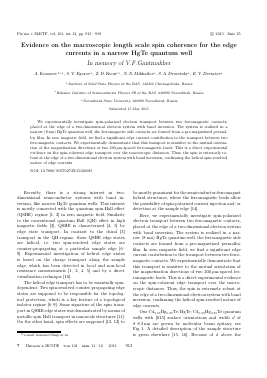
Fig. 1. (Color online) Sketch of the sample (not in scale) with electrical connections in different experimental configurations. The 100 /L/.m wide corner-shape mesa is formed by dry etching (200 nm deep) in Ar plasma. Two ferromagnetic Fe2oNigo permalloy stripes (blue, F1 and F2) are placed at the mesa step, with low (2-3 (im) overlap. In every overlap region, a side F-2DEG junction is formed between the ferromagnetic lead and the 2DEG edge. The width of each junction is equal to 20 (im. The junctions F1 and F2 are separated by the 200 (im distance along the sample edge. Several Au stripes (yellow) are placed at the mesa step, to form several normal (N) reference junctions (only N1 and N2 are shown). We use a standard two-point F-2DEG-F experimental configuration (a), realized by grounding the ferromagnetic lead F1 and using F2 to apply a current and to measure a voltage drop simultaneously. We also study electron transport across one particular F-2DEG junction (b): the corresponding ferromagnetic electrode is grounded (Fl); a current is applied between it and one of the normal contacts; two other contacts trace the 2DEG potential to both sides of the grounded junction, Vf and Vf,, respectively
critical value 6.3 nm, the quantum wells are characterized by band inversion [2, 5]. They contain a two-dimensional electron gas (2DEG) with the electron density of 1.5-1011 cnr2, as obtained from standard magnetoresistance measurements. The 2DEG mobility at 4K equals to 2 • 105 cm2/V • s.
A sample sketch is presented in Fig. la and b. The 100 ¿tm wide corner-shape mesa is formed by dry etching (200 nm deep) in Ar plasma. We fabricate F-2DEG junctions by using rf sputtering to deposit 30 nm thick ferromagnetic permalloy Fe2oNigo stripes over the mesa step, with low (2-3 ¿tni) overlap. The stripes are formed by lift-off technique, and the surface is mildly cleaned by Ar plasma before sputtering. To avoid any 2DEG
degradation, the sample is not heated during the sputtering process. The reference junctions N1 and N2 and the source-drain contacts are obtained by thermal evaporation of 100nm thick Au (yellow in Fig. 1). Without annealing procedure, only a side contact is possible between the metallic electrode and the 2DEG edge at the mesa step, because of the insulating CdTe layer on the top of the structure.
We use a standard two-point F-2DEG-F experimental configuration, realized by grounding one ferromagnetic lead and using another one to apply a current and to measure a voltage drop simultaneously, see Fig. la. We also study electron transport across one particular F-2DEG junction, see Fig. lb: the corresponding ferromagnetic electrode is grounded; a current is applied between it and one of the normal contacts; two other contacts trace the 2DEG potential to both sides of the grounded junction, V) and V&, respectively.
To obtain I—V characteristics we sweep the dc current from —1 to +lnA and measure the dc voltage in a mV range by a dc electrometer. To obtain dV/d,I(V) characteristics in Fig. 2, this dc current is additionally modulated by a low ac component (0.01 nA, 2Hz). We measure the ac dV/d.I) component of the 2DEG potential by using a lock-in with a 100 MQ input preamplifier. We have checked, that the lock-in signal is independent of the modulation frequency in the range 1-6 Hz, which is defined by applied ac filters.
The measurements are performed at a temperature of 30mK. To realize a spin-polarized transport [14], the permalloy stripes are initially pre-magnetized in the 2DEG plane. The sample is placed within a superconducting solenoid, so the initial in-plane magnetization can be changed to a normal one by introducing relatively high (above 1 T) external magnetic field. The field is switched to zero afterward, so most of the measurements are performed in zero magnetic field. Qualitatively similar results are obtained from different samples in several cooling cycles.
Fig. 2a demonstrates two-point (see Fig. fa) F-2DEG-F dV/dI(V) dependencies for both (normal and in-plane) permalloy magnetizations. In this case, we investigate in-series connected resistances of two F-2DEG junctions and a 2DEG region between them. The experimental dV/dI(V) dependencies in Fig. 2a are checked to be invariant if we exchange Ff and F2 contacts in this two-point configuration. Both curves are characterized by narrow zero-bias resistive regions and linear branches at higher biases. We do not see any effect of the magnetization direction on the zero-bias resistive region in Fig. 2a, however, it is sharply increased in an external magnetic field above 0.2 T. Thus, we should
V (mV) B (mT) V (mV)
Fig. 2. (Color online) (a) - Two-point differential resistance dV/dI(V) between two ferromagnetic leads (F1-2DEG-F2 junction) for two (normal and in-plane) permalloy magnetizations. We observe strong and narrow deeps in differential resistance, placed at ±1.16mV bias, for the permalloy film magnetization oriented within the 2DEG plane (blue line). These deeps are not seen for the normal magnetization orientation (green line), or if any of two ferromagnetic leads is changed to a normal one (N-2DEG-F configuration, dots), (b) - The external magnetic field sharply suppresses the resistance deeps at B = ±25 mT. Between B = ±25 mT, d.V/dI(B) curve demonstrates well-reproducible oscillations with a period AB ~ 10 mT. (c) - Temperature dependence of the two-point dV/dI(V) F1-2DEG-F2 curve for the in-plane permalloy magnetization in zero magnetic field. The conductance peaks at ±1.16mV bias are only weakly sensitive to the temperature below IK
connect this region with a shallow potential barrier at the F-2DEG interface, e.g. due to the proximity magnetization [17], which is fully suppressed by a temperature increase above 0.3 Iv, see Fig. 2c.
Surprisingly, we observe sharp and narrow d
Для дальнейшего прочтения статьи необходимо приобрести полный текст. Статьи высылаются в формате PDF на указанную при оплате почту. Время доставки составляет менее 10 минут. Стоимость одной статьи — 150 рублей.