ФИЗИЧЕСКАЯ ^^^^^^^^^^^^^^^^ ОПТИКА
УДК 535.34, 535.312, 539.231
EFFECT OF NANO-METRIC CHANGES ON MORPHOLOGY AND OPTICAL
CONSTANTS OF TiO2 THIN FILMS © 2014 г. S. Rafizadeh
Young Researchers Club, Urmia Branch, Islamic Azad University, Urmia, Iran E-mail: saeidrafizadeh@ieee.org Received Octover 18, 2012; in final form, March 25, 2013
Titanium dioxide films of different thicknesses, ranging from 10 to 110 nm were deposited on glass substrate, at room temperature by physical vapor deposition method. Topography, roughness and crystallography of produced layers were determined by AFM and XRD methods respectively. Optical properties were measured by transmission spectroscopy in the spectral range of 300—1100 nm wave length range. The optical constants were obtained using Kramers-Kronig analysis of the reflectivity curves. It was found that film thickness plays an important role on the nanostructures as well as optical properties of layers and cause significant variations in behavior of thin titanium oxide films.
DOI: 10.7868/S0030403414010188
1. INTRODUCTION
TiO2 is one of the most widely studied ceramic materials used as films. These films are frequently employed for many optical devices in optics industry (Pulker, 1999), dye-sensitized solar cells (Sung and Kim, 2007), heat mirrors (Okada et al., 2006) and environmental applications (Fujishima et al., 2000) for their remarkable optical, photocatalytic and hydro-
philic properties. TiO2 films also possess noble antibacterial, disinfection, antifogging and self-cleaning properties (Sun et al., 2008) [1]. TiO2 is known to exist in an amorphous form and to crystallize in three distinct structures: two tetragonal phases, anatase (a = = 0.3785 nm, c = 0.9514 nm) and rutile (a = 0.4593 nm, c = 0.2959 nm), and a third orthorhombic phase, brookite (a = 0.5456 nm, b = 0.9182 nm, c = 0.5143 nm)
Roughness, nm 40 г
30 -
20 -
10 -
_i_i_i_i_i_i
0 20 40 60 80 100 120
Thickness, nm
Fig. 2. The roughness curve of produced TiO2/glass layers at room temperature.
in which a,b and c define the crystallographic directions and the lattice constants of the phases [2]. Many techniques can be used to deposit TiO2 films. They include physical vapor deposition method [3], sol gel process [4], chemical vapor deposition [5], ion-assisted deposition [6], and sputtering [7]. Film thickness, deposition rate, and method of coating play important role on microstructure as well as macroscopic properties of films [8, 9]. In this work, the behavior of thin titanium oxide films of different thicknesses deposited on glass substrate at room temperature, by physical vapor deposition method is studied.
2. EXPERIMENTAL DETAILS
Titanium dioxide films of different thicknesses, at normal deposition angle, deposited on glass substrates (18 x 18 x 1 mm cut from microscope slide) by resistive evaporation from tungsten boats at room temperature. The purity of titanium dioxide powder was 98%.
An ETS 160 (Vacuum Evaporation System User Manual) coating plant with a base pressure of 3 x 10⁻⁵ mbar was used. Prior to deposition, all glass substrates were ultrasonically cleaned in heated acetone (within 15 min) then ethanol (within 15 min). The substrate holder was a disk of 36.5 cm in diameter with adjustable height up to 50 cm and also adjustable keepers for placing any kind of substrates. The distance between the center of the evaporation boat and the center of the substrate was 45 cm. Thickness of layers were determined by quartz crystal technique and other deposition conditions such as deposition rate, vacuum pressure, and substrate temperature was the same in all layers. The nanostructure of these films was obtained using a Philips XRD X'pert MPD Diffractometer (CuKa radiation) with a step size of 0.03 and count time of1 s per step, while the surface physical morphology and roughness were obtained by means of AFM (Dual Scope TM DS 95-200/50) analysis. Transmittance of the films was measured using UV-VIS spectrophotometer (Hitachi U — 3310) instrument. The spectrum of the layers were in the range of 300—1100 nm wave length (UV-VIS), and for using Kramers-Kronig relations [10], we extrapolated the rest of reflectivity curves with Rao [11] data, he just reported reflectance of TiO2 layers in long wave length range. The optical properties such as real part of refractive index (n), extinction coefficient (k), real part of dielectric constant (st), imaginary part of dielectric constant (s2), absorption coefficient (a) and bandgap energy were obtained and compared with Ribarsky [12] results.
3. RESULT AND DISCUSSION 3.1. Structural Analysis
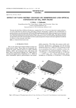
Figure 1 shows AFM images for TiO2/glass thin layers of different thicknesses produced in this work. As it can be seen from Fig. 1a, for 10 nm thickness, there are few needle like grain on surface and mor-
10 30 50 70 90
29, deg
Fig. 3. The XRD pattern of TiO2/glass layers with 10 nm, 40 nm, 70 nm, 110 nm thickness at room temperature.
R
E, eV
Fig. 4. Reflectivity curve TiO^glass layers of different thicknesses at room temperature.
Fig. 5. Real part of refractive index vs. energy for different film thicknesses of TiO^glass layers at room temperature.
phology of this layer (d = 10 nm) is almost the same as glass substrate. By increasing thickness, layers get more completed, in Fig. 1b, for 40 nm thickness, surface is full of needle like grains and by increasing thickness to 70 nm, as it can be seen from Fig. 1c, needle like grains change to small domed grains. Figure 1d shows TiO2/glass layer with 110 nm thickness, as it can be seen the layer is more completed and there are big domed grains on the surface, and surface seems rougher. For the layers produced in this work, we are encountered with Zone I of structure zone model [13],
the region consisting of domed top tapered structure with voids between them, that is because ofTs/Tm = 0.17 (Ts is substrate temperature and Tm is melting temperature) and is obvious from AFM images. Figure 2 shows roughness curve for TiO2/glass thin layers produced in this work as it can be seen, by increasing thickness and forming big domed grains, roughness increases. There is a decrease from 10 nm to 40 nm thickness, that is because 50 nm layer is more completed, and surface is smoother, which is in agreement with Fig. 1b. Figure 3 shows XRD patterns for
1.26
1.76
2.26
2.76
3.26
3.76 E, eV
Fig. 6. Imaginary part of refractive index vs. energy for different film thicknesses of TiO2/glass layers at room temperature.
TiO^glass thin layers of different thicknesses produced in this work. As it can be seen from Figs. 3a and 3b, for both 10 nm and 40 nm thicknesses respectively, there are no crystallographic directions and layers are amorphous. By increasing thickness to 70 nm, layer get more completed and there is a small A(004) crys-tallographic direction at almost 29 = 38°, and by increasing thickness to 110 nm, the same peak A(004)
becomes clear and sharp. So thickness play an important role on crystallographic directions and XRD patterns, for the layers produced in this work. A wide peak at 29 = 15° also noisy XRD patterns, depend to amorphous glass substrate. Figure 4 shows reflectivity curves in VIS light wave length (1 eV up to 4 eV energy range) for TiO2/glass layers of different thicknesses and the same other deposition conditions. As it can be seen by increasing thickness, there is an increasing trend for reflectivity curve and that is because, layers get more completed which is in agreement with Fig. 1 (AFM images). The fraction of voids decrease and there for reflectivity increases.
3.2. Optical Analysis
Using Kramers-Kronig relations on reflectivity curves (as mentioned before), optical constant were calculated for the layers produced in this work. Figure 5 shows real part of refractive index (n). Rebarskys data is also included for comparison. As it can be seen, the general trend of our results are the same as Rebarskys. There are two peaks for Rebarskys result, at 2.6 eV and 3.6 eV energies, these peaks for our results are at 1.4 eV and 3.6 eV energies. The first small peak has been shifted back at about 1.5 eV energy, that depends to deposition conditions and deposition method. By increasing thickness and formation of big cluster, layer get un uniform and real part of refractive index (n), increases, that is in agreement with AFM images (Fig. 1). Because of gettering property of Ti and low thickness of 10 nm TiO2/glass layer, related curve cross other curves and showed an energy dependence. Figure 6 shows imaginary part of refractive index (k). Reberskys
k
3
Fig. 7. Real part of dielectric constants for TiO2/glass films of different thicknesses at room temperature.
Fig. 8. Imaginary part of dielectric constants for TiO^glass films of different thicknesses at room temperature.
data is also included for comparison. The general trend of our results is the same as Reharskys result. There is a bump at 3.2 eV energy and a big peak at 4.2 eV energy for Reharskys data.The bump for our results, is at 1.15 eV energy for all layers and at 3.6 eV energy for 10 nm thickness. The second big peak is at 3.9 eV energy for all layers and at 4 eV energy for 10 nm thickness, that is exactly in agreement with Reharskys result. Gettering property of Ti during increasing
thickness process, tends to some changes in curves for our results. As it can be seen from Fig. 6, more complete layers produced and the fraction of voids decreases, there for transmittance decreases and extinction coefficient (k) increases.
Figure 7, shows real part of dielectric constant (s1). Rebarskys result is also added for comparison. The general trend of our results are as same as Reharskys result. There is a small peak at 2.6 eV energy and a big one at 3.6 eV energy for Reharskys data. The first peak appear at 3.5 eV energy for all layers and at 3.8 eV energy for 10 nm thickness. By increasing thickness, completed semiconductor layers of TiO2
Для дальнейшего прочтения статьи необходимо приобрести полный текст. Статьи высылаются в формате PDF на указанную при оплате почту. Время доставки составляет менее 10 минут. Стоимость одной статьи — 150 рублей.